Display device
a technology of display device and display pixel, which is applied in the direction of thermoelectric devices, organic semiconductor devices, solid-state devices, etc., can solve the problems of local brightness unevenness in the same light-emitting pixel, reduction of luminous efficiency of elements, and deterioration of color purity, so as to improve luminous efficiency and color purity.
- Summary
- Abstract
- Description
- Claims
- Application Information
AI Technical Summary
Benefits of technology
Problems solved by technology
Method used
Image

Examples
first embodiment
(1) First Embodiment
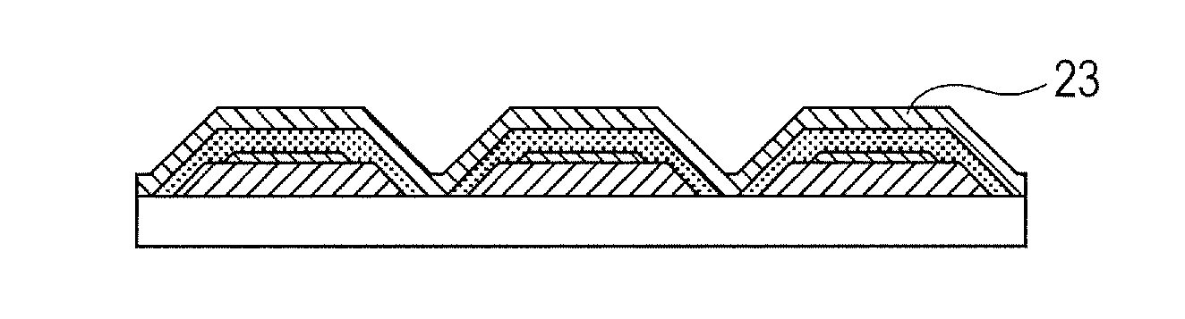
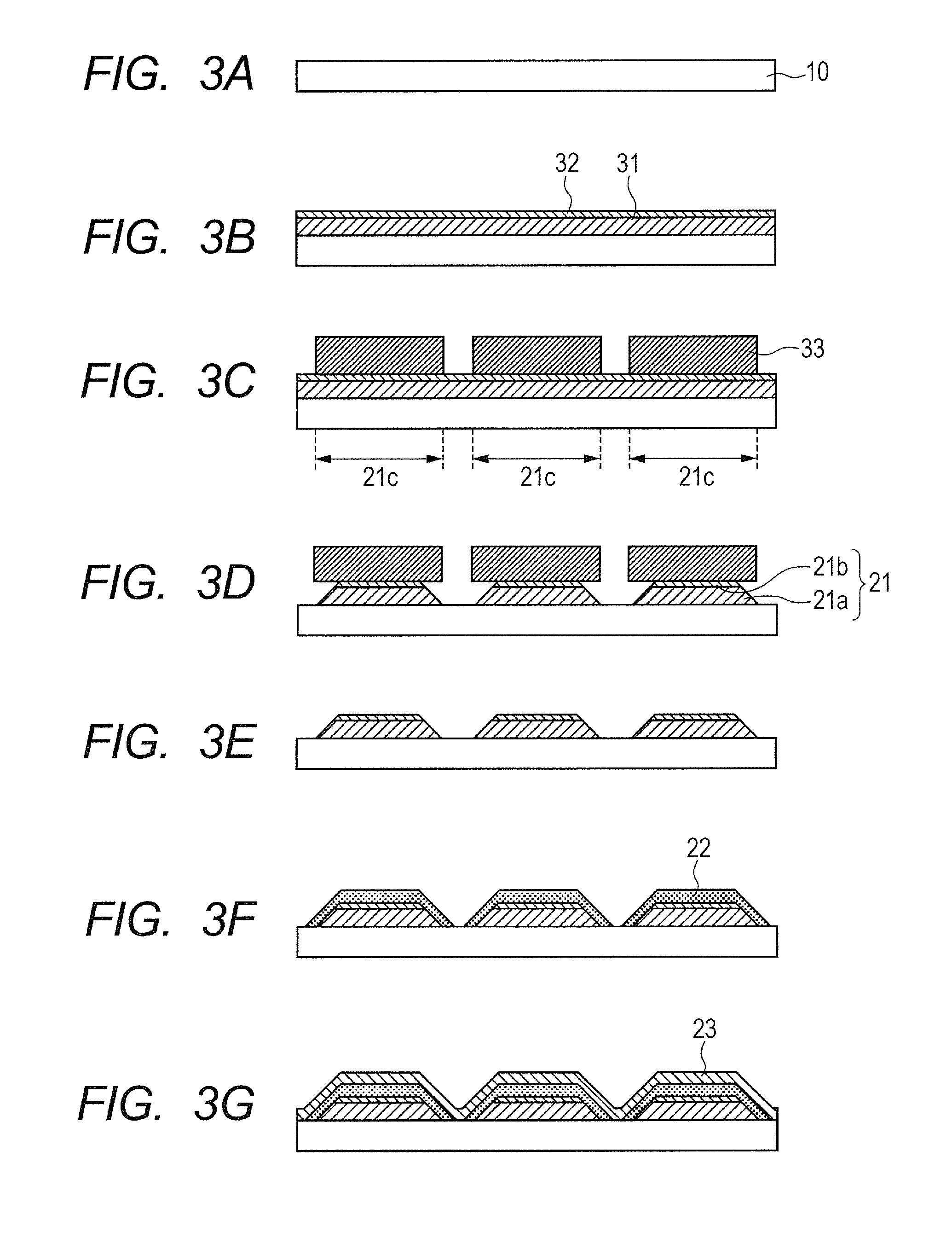
[0024]FIG. 1 is a schematic sectional view illustrating a display device according to First Embodiment of the present invention. A display device 1 of FIG. 1 includes, on a substrate 10, multiple (three) organic EL elements 20 each constituted of the lower electrode 21 provided on the substrate 10, the organic compound layer 22, and an upper electrode 23. In the display device 1 of FIG. 1, the lower electrode 21 is provided by laminating a first lower electrode layer 21a and a second lower electrode layer 21b from a side closer to the substrate 10 in the stated order.
[0025]By the way, the display device 1 of FIG. 1 is an organic EL display device having the organic EL elements 20, but in the present invention, the display elements constituting the display device may be changed to light-emitting elements except the organic EL elements 20 such as inorganic EL elements.
[0026]Next, a constituent layer for the display device 1 of FIG. 1 is described.
[0027]Any substrate c
second embodiment
(2) Second Embodiment
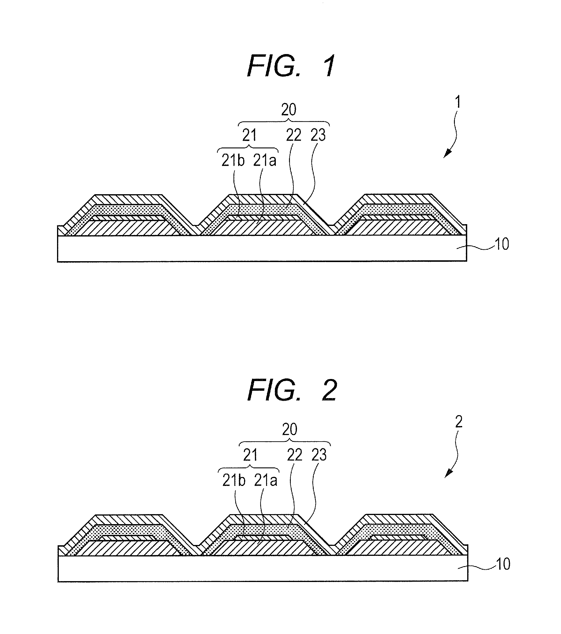
[0052]FIG. 2 is a schematic sectional view illustrating a display device according to Second Embodiment of the present invention. In a display device 2 of FIG. 2, the same component as that of the display device 1 of FIG. 1 is represented by the same reference symbol. As compared with the display device 1 of FIG. 1, the display device 2 of FIG. 2 is different from the display device 1 of FIG. 1 in that a lower end portion of the second lower electrode layer 21b is placed in a plane region so as not to coincide with an upper end portion of the first lower electrode layer 21a.
[0053]Here, the first lower electrode layer 21a and the second lower electrode layer 21b illustrated in FIG. 2 are each individually formed by using a photolithography process (a processing process for an electrode layer formed of a photolithography method and etching). In other words, the lower electrode 21 constituting the display device of this embodiment is formed by using the photolithogra
third embodiment
(3) Third Embodiment
[0054]In the display device of the present invention, the step of treating the surface of the lower electrode 21 may be provided between the performance of patterning based on the photolithography process after the formation of the lower electrode 21 and the initiation of the formation of the organic compound layer 22.
[0055]Here, a method of treating the surface of the lower electrode 21 is, for example, a surface treatment involving using phosphoric acid (phosphoric acid treatment) or a surface treatment involving using oxygen turned into plasma (O2 plasma treatment).
[0056]Here, part of the electrode materials listed in Table 1 were subjected to an experiment concerning a surface treatment for the lower electrode 21.
[0057]Specifically, first, a lower electrode was formed with an electrode material shown in Table 4 below. After that, the lower electrode was subjected to the following surface treatments.
[0058](A) Phosphoric Acid Treatment
[0059]An 11% aqueous solution
PUM
 Abstract
Description
Claims
Application Information
 - R&D Engineer
- R&D Manager
- IP Professional
- Industry Leading Data Capabilities
- Powerful AI technology
- Patent DNA Extraction
Browse by: Latest US Patents, China's latest patents, Technical Efficacy Thesaurus, Application Domain, Technology Topic.
© 2024 PatSnap. All rights reserved.Legal|Privacy policy|Modern Slavery Act Transparency Statement|Sitemap