Display Device and Method of Manufacturing Thin Film Transistor
- Summary
- Abstract
- Description
- Claims
- Application Information
AI Technical Summary
Benefits of technology
Problems solved by technology
Method used
Image

Examples
Example
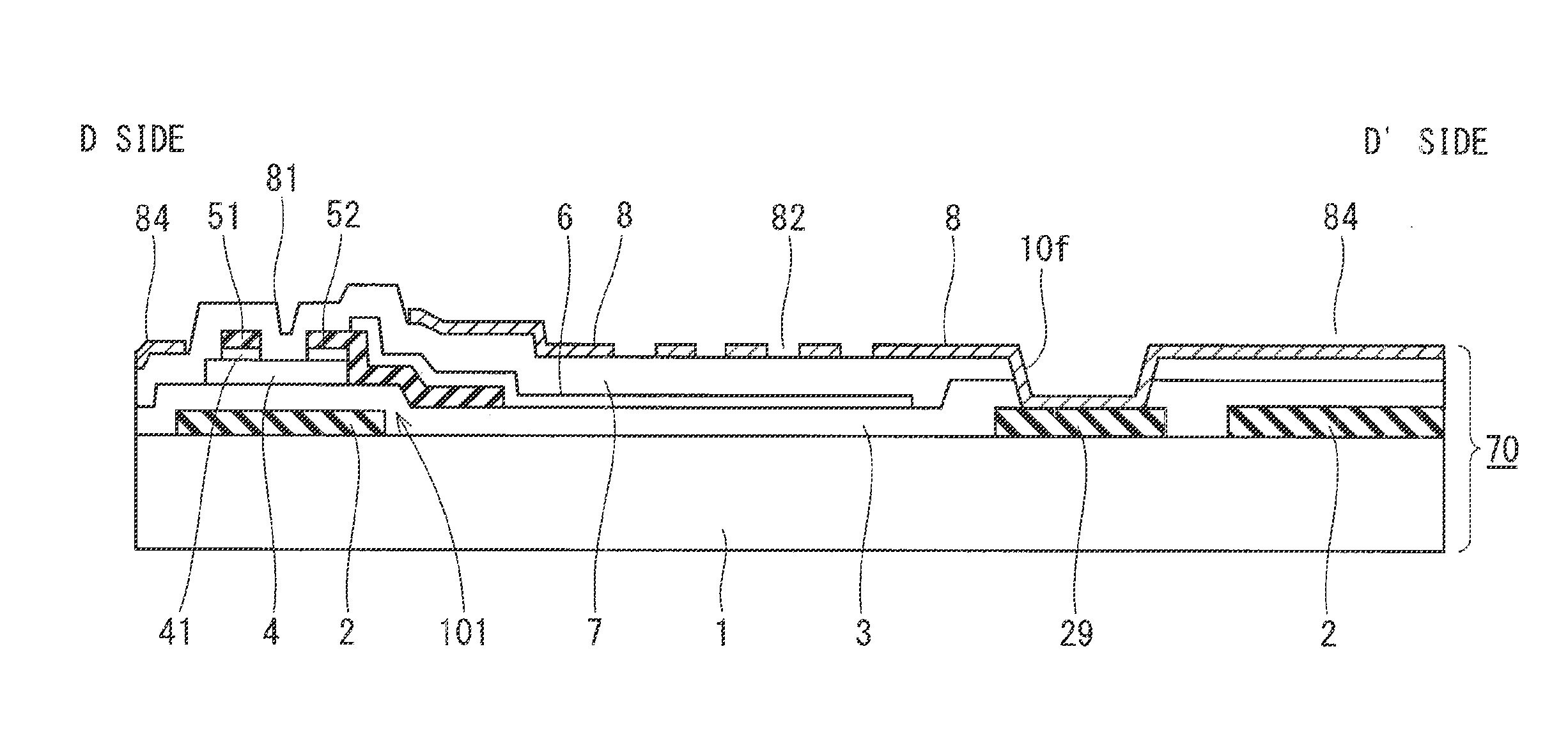
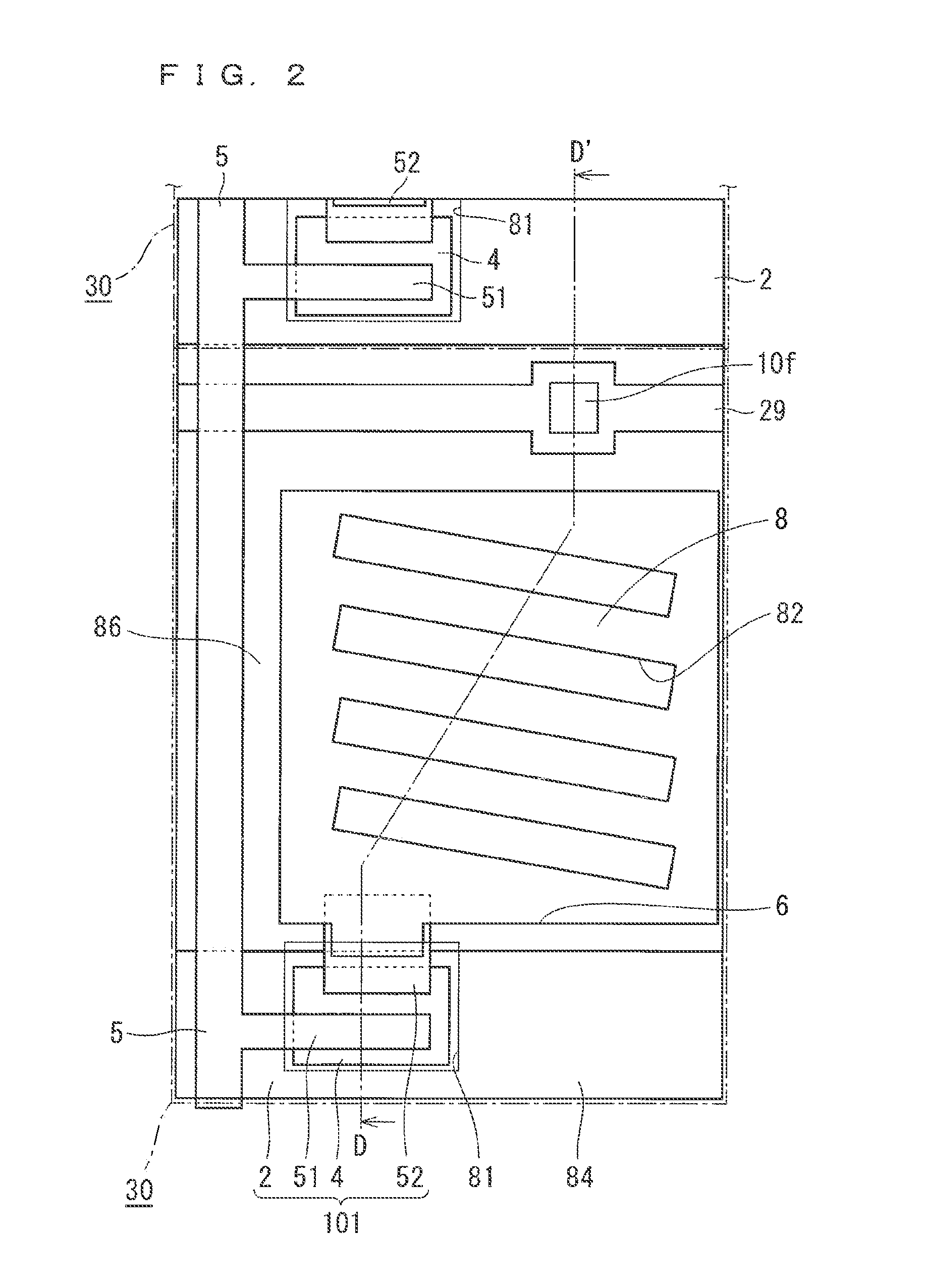
[0125]In the structure of the first embodiment, after the gate insulating film 3, the semiconductor films 4, 42, and 43, and the ohmic contact film 41 are layered, adopted is a process for forming an opening in the gate insulating film 3 by using a photomask used for forming the contact holes 9a and 9b. After that, the source wire 5, the wire 53, and the electrodes 55 and 56 are formed. The film which is formed in the same process as that of the connection portion 86 and the shield electrode 90 is not thereby needed to connect the gate wire 2 and the gate-wire leading line 14 to another wire.
[0126]Therefore, as described above, with the shield electrode 90, it is possible to shield the electric field generated from the gate wire 2 without widening the frame area. The above can be generally described as follows: The liquid crystal display shown in the first embodiment is a display device having the liquid crystal display panel 60. The liquid crystal display panel 60 includes the array s
Example
The Second Embodiment
[0140]In the second embodiment of the present invention, a preferred method of forming the wire 53 and the electrode 55, and the source electrode 51 and the drain electrode 52 in the same process will be described. More specifically, a photomask used for forming the contact hole 9a or 9b is made common to a photomask used for forming the semiconductor film 4.
[0141]The structure obtained by the manufacturing method described in the second embodiment is the same as that shown in the first embodiment, and therefore the second embodiment produces the same effect as that of the first embodiment, for increasing display quality without widening the frame area.
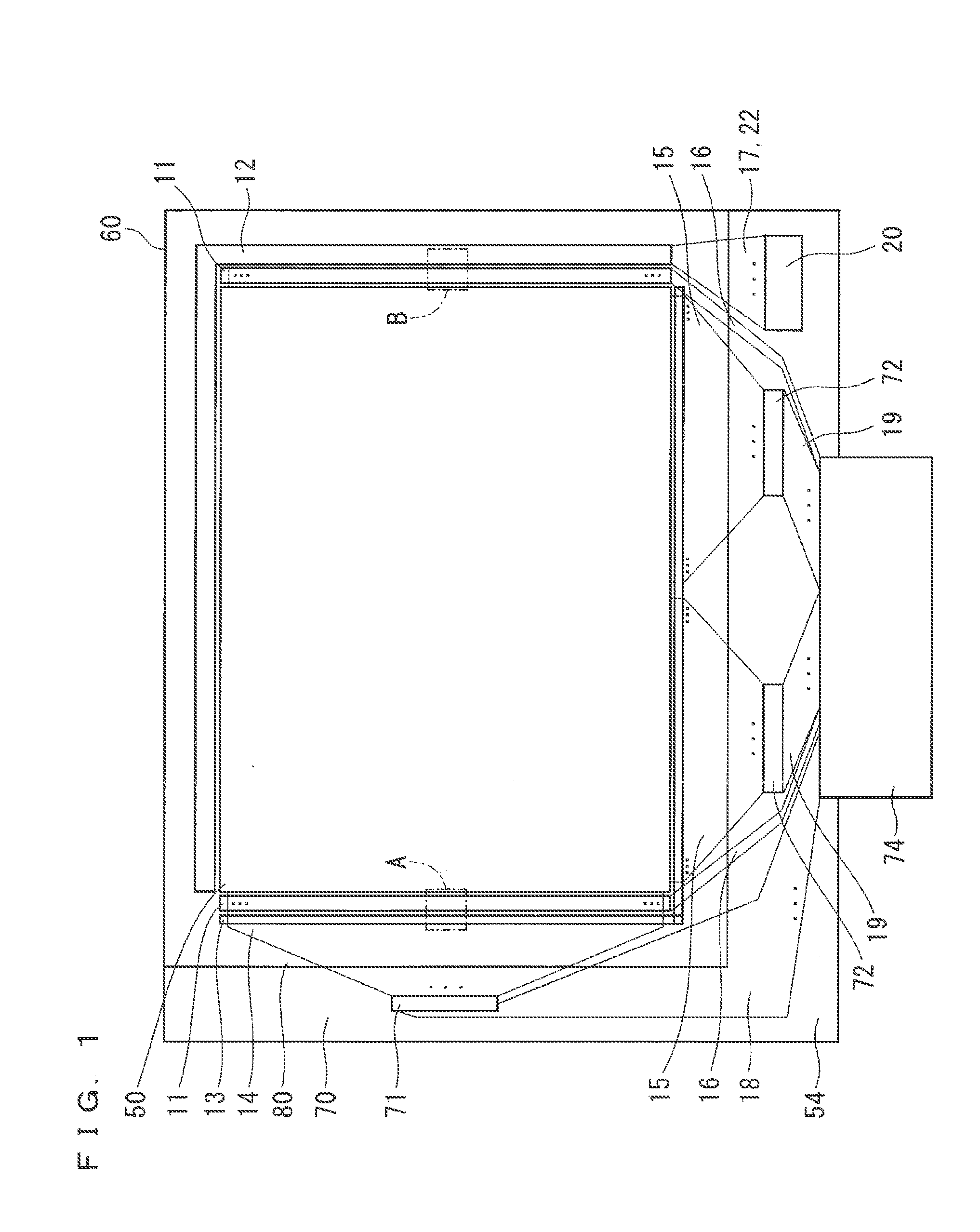
[0142]FIGS. 9 to 16 are cross sections used for explanation of a flow of manufacturing process of a display device in accordance with the second embodiment. In these figures, on the left side of the break line, shown is a cross section of an area where the TFT 101 (see FIGS. 1 and 3) is to be formed, and on the right
PUM
 Abstract
Description
Claims
Application Information
 - R&D Engineer
- R&D Manager
- IP Professional
- Industry Leading Data Capabilities
- Powerful AI technology
- Patent DNA Extraction
Browse by: Latest US Patents, China's latest patents, Technical Efficacy Thesaurus, Application Domain, Technology Topic.
© 2024 PatSnap. All rights reserved.Legal|Privacy policy|Modern Slavery Act Transparency Statement|Sitemap