Circuit board and on-board structure of semiconductor integrated circuit
- Summary
- Abstract
- Description
- Claims
- Application Information
AI Technical Summary
Benefits of technology
Problems solved by technology
Method used
Image

Examples
first preferred embodiment
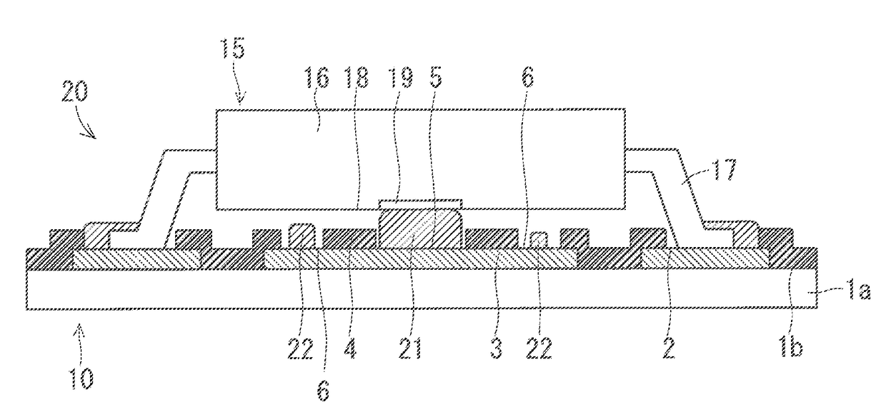
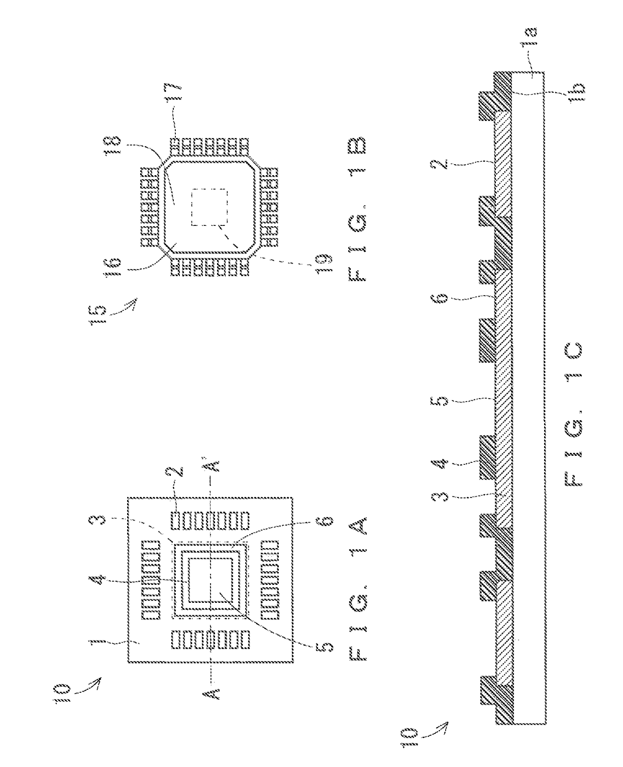
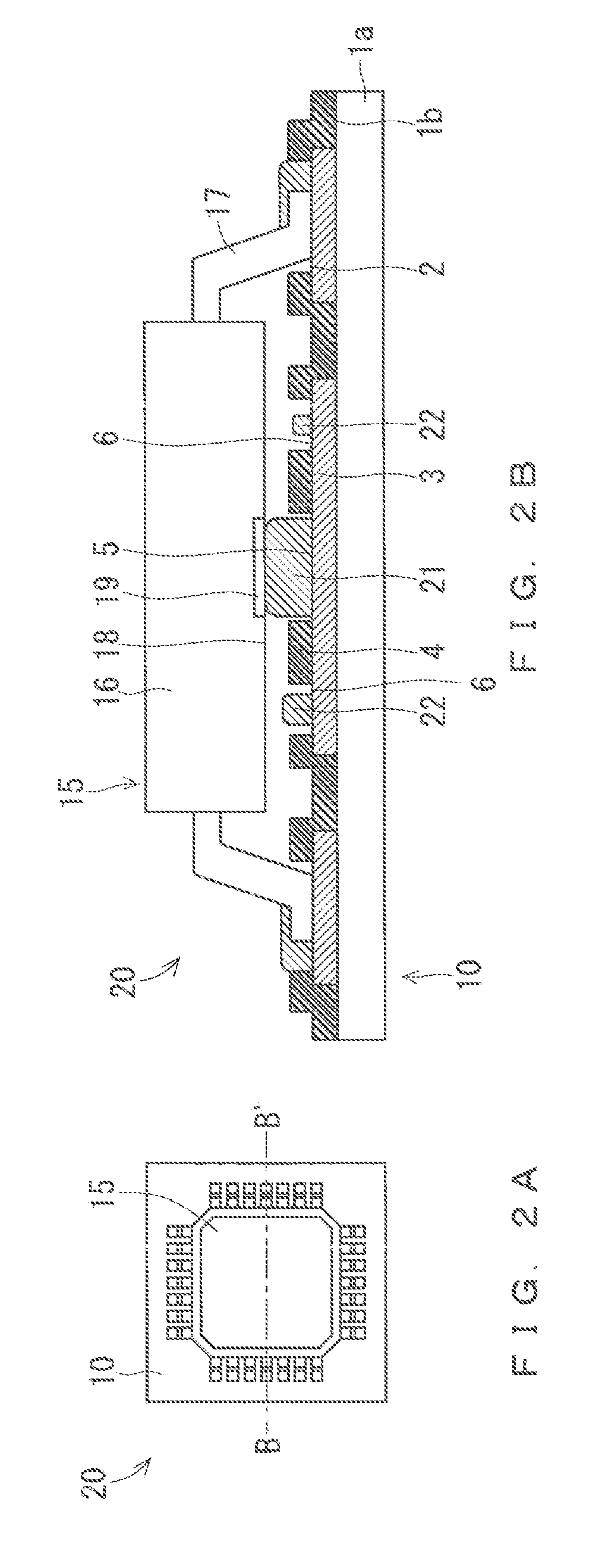
[0019]FIG. 1A is a plan view of the circuit board 10 in a first preferred embodiment.
[0020]FIG. 1B is a plan view of a semiconductor IC circuit 15 in the first preferred embodiment. FIG. 1C is a cross-sectional view of the circuit board 10 taken along the line A-A′ of FIG. 1A.
[0021]As illustrated in FIG. 1B, the semiconductor IC circuit 15 includes a package body 16 that accommodates a semiconductor chip (not shown) and terminals 17 aligned along at least part of the periphery of the package body 16. The semiconductor IC circuit 15 is a circuit of the surface-mounted quad flat package (QFP) type, with a plurality of leads, namely, the terminals 17 aligned along the four sides of the package body 16.
[0022]The semiconductor IC circuit 15 also includes a heat-dissipating unit 19 located in the rear surface thereof, or, in a joint surface 18 (see FIG. 2B), which faces the circuit board 10 having the semiconductor IC circuit 15 mounted thereon. The heat-dissipating unit 19 is to be joined t
second preferred embodiment
[0042]The following will describe the circuit board 10 and the on-board structure 20 of the semiconductor IC circuit 15 according to a second preferred embodiment. The configuration and operation similar to those described in the first preferred embodiment will not be further elaborated here.
[0043]FIG. 3 is a plan view of the circuit board 10 in the second preferred embodiment. The circuit board 10 includes second open areas 7 as well as the heat-dissipating connection pad 5 and the first open area 6 mentioned in the first preferred embodiment. In the individual second open area 7, the metal layer 3 is exposed as the outermost layer of the substrate 1 from an opening in the insulating layer 4 located between the heat-dissipating connection pad 5 and the first open area 6. One end of the individual second open area 7 is connected to the heat-dissipating connection pad 5, whereas the other end is connected to the first open area 6. In the second preferred embodiment, each of the second o
third preferred embodiment
[0047]The following will describe the circuit board 10 and the on-board structure 20 of the semiconductor IC circuit 15 according to a third preferred embodiment. The configuration and operation similar to those described in the first preferred embodiment will not be further elaborated here.
[0048]FIG. 4 is a plan view of the circuit board 10 in the third preferred embodiment. The circuit board 10 includes the heat-dissipating connection pad 5 shaped in an octagon. The circuit board 10 also includes the second open areas 7, each of which is a triangle whose base is one of the eight sides of the octagonal heat-dissipating connection pad 5 and is opposed to the base of another triangle, with the apex of each triangle located on a radial line extending from the center of the octagon. In addition, the circuit board 10 includes the first open areas 6, each of which is a circle whose arc includes the apex of the corresponding one of the triangles. Each of the triangular second open areas 7 is
PUM
 Abstract
Description
Claims
Application Information
 - R&D Engineer
- R&D Manager
- IP Professional
- Industry Leading Data Capabilities
- Powerful AI technology
- Patent DNA Extraction
Browse by: Latest US Patents, China's latest patents, Technical Efficacy Thesaurus, Application Domain, Technology Topic.
© 2024 PatSnap. All rights reserved.Legal|Privacy policy|Modern Slavery Act Transparency Statement|Sitemap