Resistive element and method of manufacturing the resistive element
- Summary
- Abstract
- Description
- Claims
- Application Information
AI Technical Summary
Benefits of technology
Problems solved by technology
Method used
Image

Examples
first modified example
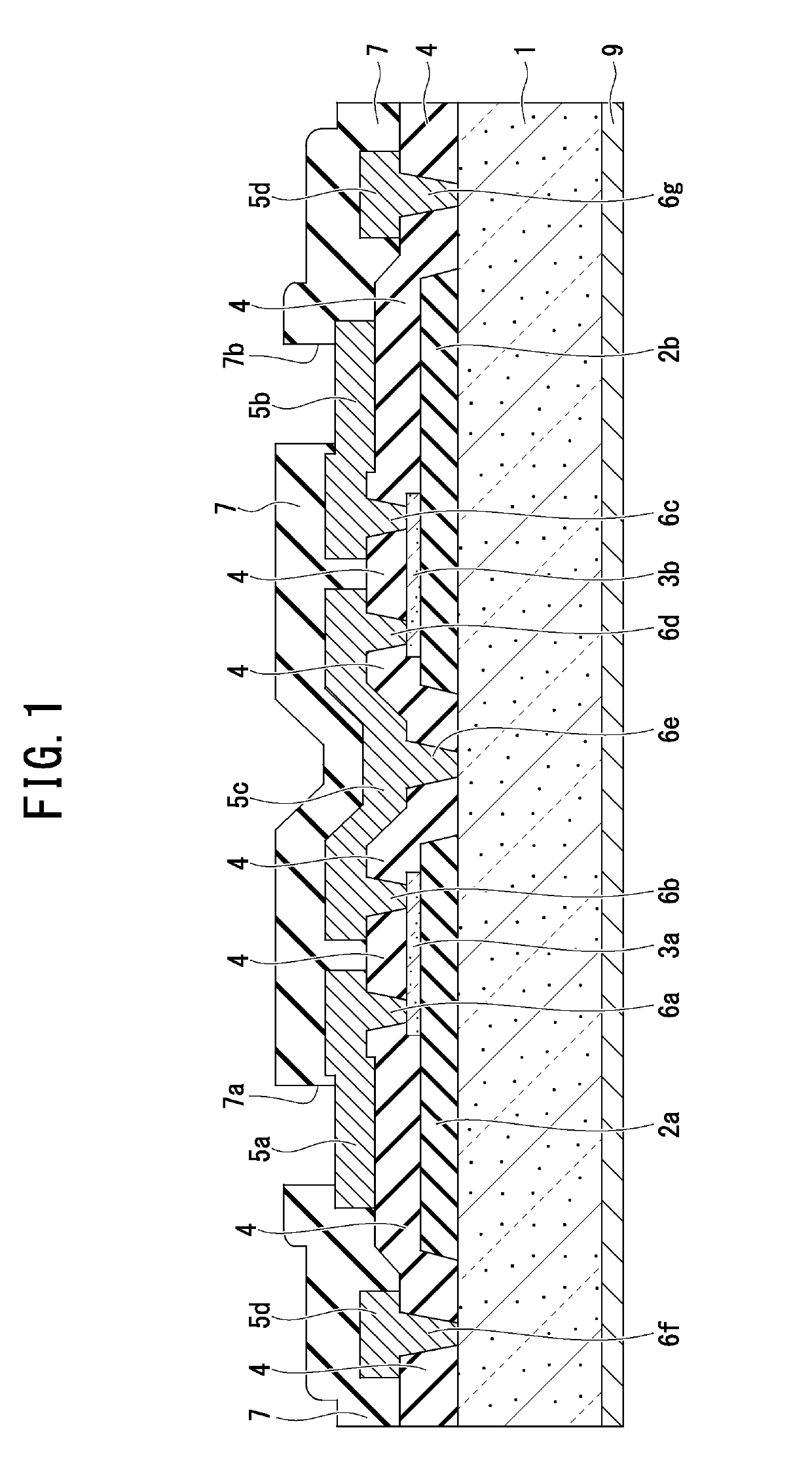
[0073]A resistive element according to a first modified example of the embodiment of the present invention illustrated in FIG. 20 differs from the resistive element illustrated in FIG. 1 in further including auxiliary films 3c and 3d in a floating state in terms of potential allocated on the first insulating films 2a and 2b and separated from the resistive layers 3a and 3b.
[0074]The auxiliary film 3c is deposited below the first electrode 5a of the paired first electrodes 5a and 5b and separated from the resistive layer 3a. The auxiliary film 3d is deposited below the other first electrode 5b and separated from the resistive layer 3b. The auxiliary films 3c and 3d are made of the same material as the resistive layers 3a and 3b, such as n-type doped polysilicon, and have the same thickness as the resistive layers 3a and 3b. The auxiliary films 3c and 3d have a rectangular planar pattern, for example. The other structures in the resistive element according to the first modified example
second modified example
[0077]The resistive element according to the embodiment of the present invention described above includes the plural first insulating films 2a and 2b, resistive layers 3a and 3b, and first electrodes 5a and 5b, and the single relay wire 5c electrically connected to each one end of the resistive layers 3a and 3b, as illustrated in FIG. 1. A resistive element according to a second modified example of the embodiment of the present invention illustrated in FIG. 21 differs from the resistive element illustrated FIG. 1 in including a plurality of resistive layers 3a and 3b and relay wires 5f and 5g, and a single first electrode 5e electrically connected to each one end of the resistive layers 3a and 3b.
[0078]An auxiliary film 3e in a floating state in terms of potential is deposited on a first insulating film 2c and separated from the resistive layers 3a and 3b so as to be interposed between the resistive layers 3a and 3b. The auxiliary layer 3e is made of the same material as the resistive
PUM
 Abstract
Description
Claims
Application Information
 - R&D Engineer
- R&D Manager
- IP Professional
- Industry Leading Data Capabilities
- Powerful AI technology
- Patent DNA Extraction
Browse by: Latest US Patents, China's latest patents, Technical Efficacy Thesaurus, Application Domain, Technology Topic.
© 2024 PatSnap. All rights reserved.Legal|Privacy policy|Modern Slavery Act Transparency Statement|Sitemap