Method for designing layout of semiconductor device and method for manufacturing semiconductor device using the same

a semiconductor device and layout design technology, applied in the direction of cad circuit design, semiconductor/solid-state device details, instruments, etc., can solve the problems of significant time, trial and error, and design a layout of a semiconductor device using a layout design tool, and achieve the effect of reducing the layout design tim

Active Publication Date: 2019-10-10
SAMSUNG ELECTRONICS CO LTD
View PDF0 Cites 1 Cited by
  • Summary
  • Abstract
  • Description
  • Claims
  • Application Information

AI Technical Summary

Benefits of technology

The invention provides methods for quickly creating new designs on electronic devices by inserting small cells into them without having to manually adjust any changes that may affect their performance or functionality during manufacturing processes. This results in faster production times while improving efficiency compared with traditional techniques such as trial-and-error testing.

Problems solved by technology

The technical problem addressed in this patented text relates how to efficiently create high-density integrated circuits (ICs) with smaller sizes while maintaining their functionality or performance at competitive prices. This can be achieved by optimizing the placement of components within each circuit layer on top of another circuit layer during production.

Method used


Image

  • Method for designing layout of semiconductor device and method for manufacturing semiconductor device using the same
  • Method for designing layout of semiconductor device and method for manufacturing semiconductor device using the same
  • Method for designing layout of semiconductor device and method for manufacturing semiconductor device using the same

Examples


Embodiment Construction

[0032]It is to be understood that both the foregoing general description and the following detailed description are provided as examples, for illustration and not for limiting the scope of the inventive concept. Reference will now be made in detail to the exemplary embodiments, which are illustrated in the accompanying drawings. Wherever possible, the same reference numbers are used in the drawings and the description to refer to the same or like parts.

[0033]It will be understood that when an element is referred to as being “connected,” or “coupled,” to another element or layer, it can be directly connected or coupled to the other element or intervening elements may be present. In contrast, when an element is referred to as being “directly connected,” or “directly coupled,” to another element, there are no intervening elements present. As used herein, the term “and / or,” includes any and all combinations of one or more of the associated listed items.

[0034]Although the terms first, sec


PUM


Abstract

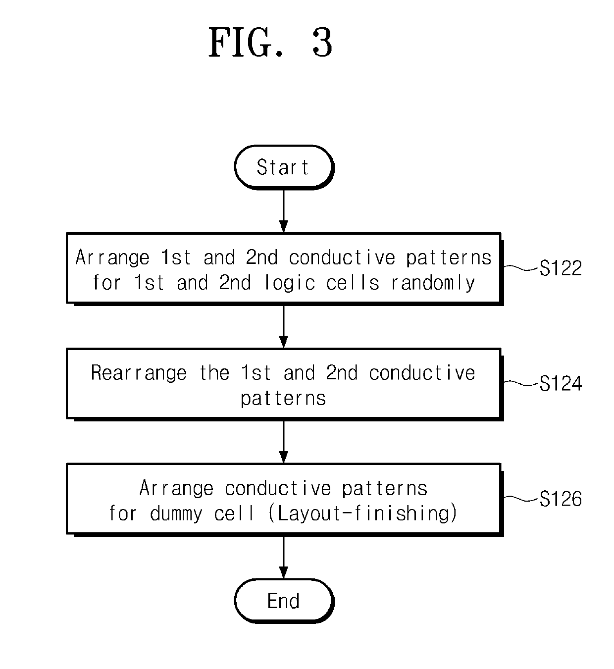
A method of manufacturing a semiconductor device includes configuring a layout pattern; and forming conductive lines corresponding to the layout pattern on a substrate, wherein configuring the layout pattern includes: arranging pre-conductive patterns and post-conductive patterns for a first logic cell, a second logic cell, and a third logic cell; rearranging the pre-conductive patterns and the post-conductive patterns so that two conductive patterns that are adjacent to a boundary between two adjacent logic cells from among the first logic cell, the second logic cell, and the third logic cell are formed by different photolithography processes; and arranging conductive patterns for a dummy cell arranged between the second logic cell and the third logic cell.

Description


Claims


Application Information

Patent Timeline
Owner SAMSUNG ELECTRONICS CO LTD
Why Eureka
Try Eureka