Circuits and methods for preventing bias temperature instability
a technology of bias temperature instability and circuits, applied in the field of circuits, can solve the problems of reducing the drain current increasing the threshold voltage of the cmos transistor, and negatively affecting the performance of the device in which the cmos transistor is provided,
- Summary
- Abstract
- Description
- Claims
- Application Information
AI Technical Summary
Benefits of technology
Problems solved by technology
Method used
Image

Examples
Embodiment Construction
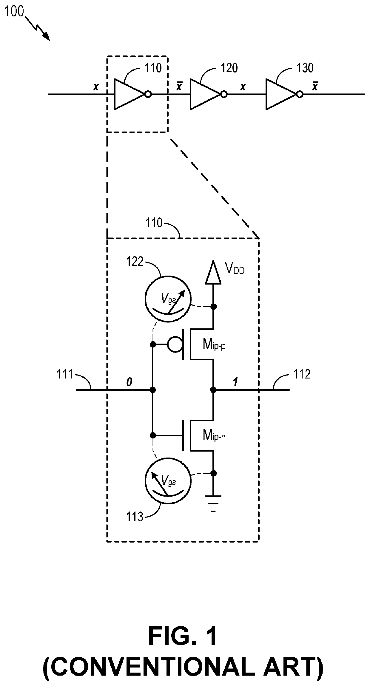
[0019]As noted above, current techniques to combat BTI degradation include provision of higher supply voltages to the affected CMOS transistor (to power through the increased threshold voltage and pump up the drain current), increased timing margins (to decrease the sensitivity of the circuit to BTI degradation of the CMOS transistor), and clock toggling (to decrease the imbalance between ON periods and OFF periods experienced by the CMOS transistor). However, each of these techniques has serious drawbacks.
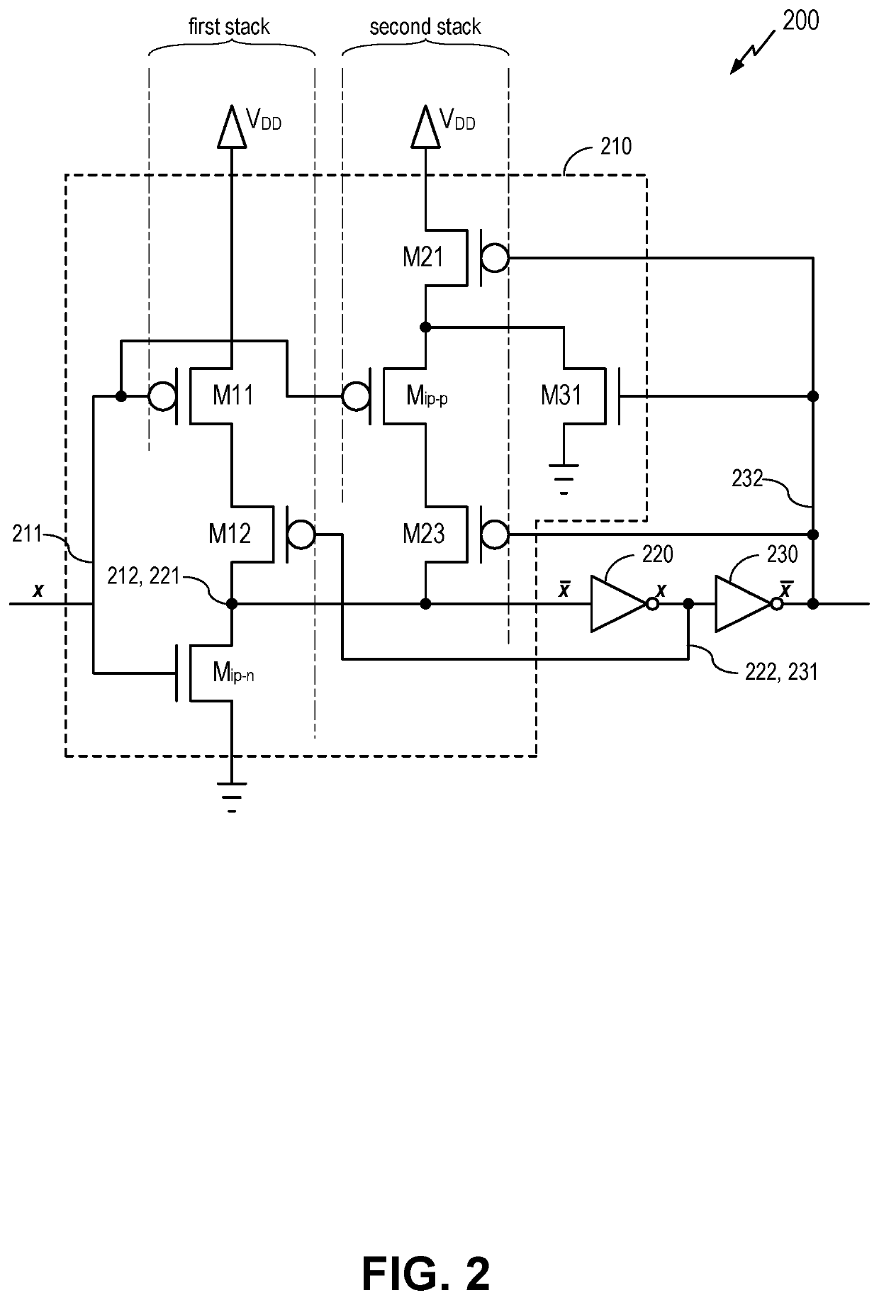
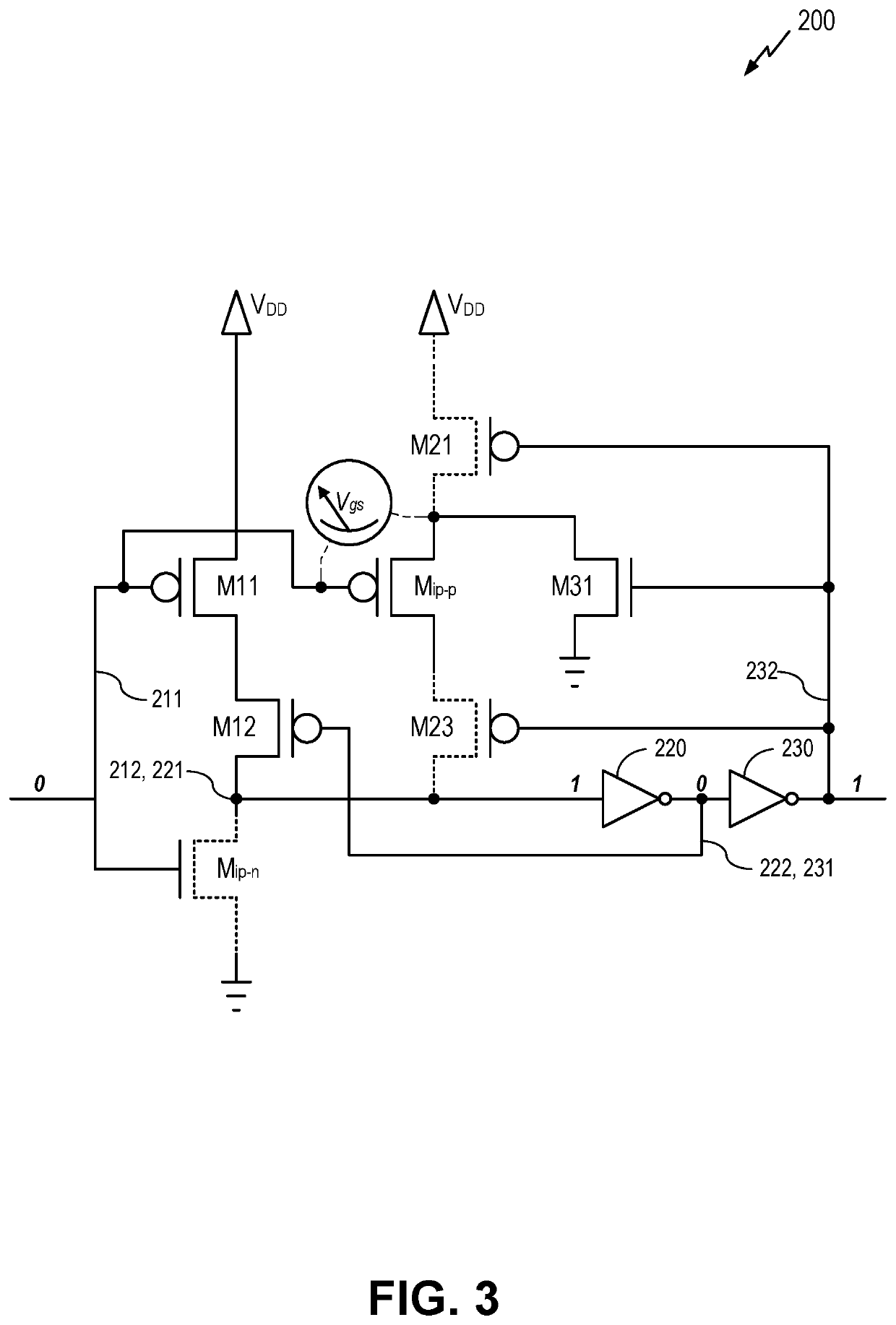
[0020]Accordingly, in accordance with aspects of the disclosure, a PMOS-protected inverter structure is proposed. The inverter may have an inverter pair PMOS and an inverter pair NMOS. To prevent BTI degradation of the inverter pair PMOS, a balancing transistor may be provided to balance a voltage at a source of the inverter pair PMOS. The balancing may be performed in response to receiving of a low voltage at an input node of the inverter structure, i.e., the gates of the inverter p
PUM
 Abstract
Description
Claims
Application Information
 - R&D Engineer
- R&D Manager
- IP Professional
- Industry Leading Data Capabilities
- Powerful AI technology
- Patent DNA Extraction
Browse by: Latest US Patents, China's latest patents, Technical Efficacy Thesaurus, Application Domain, Technology Topic.
© 2024 PatSnap. All rights reserved.Legal|Privacy policy|Modern Slavery Act Transparency Statement|Sitemap