Method of etching dual damascene structure
a damascene and etching technology, applied in the field of etching methods, can solve the problems that silkTM, the low-k film material, and the resist cannot be mixed together, and achieve the effect of maintaining dimensional stability
- Summary
- Abstract
- Description
- Claims
- Application Information
AI Technical Summary
Benefits of technology
Problems solved by technology
Method used
Image

Examples
first embodiment
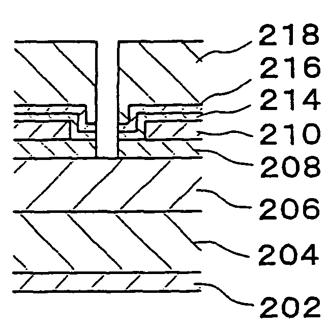
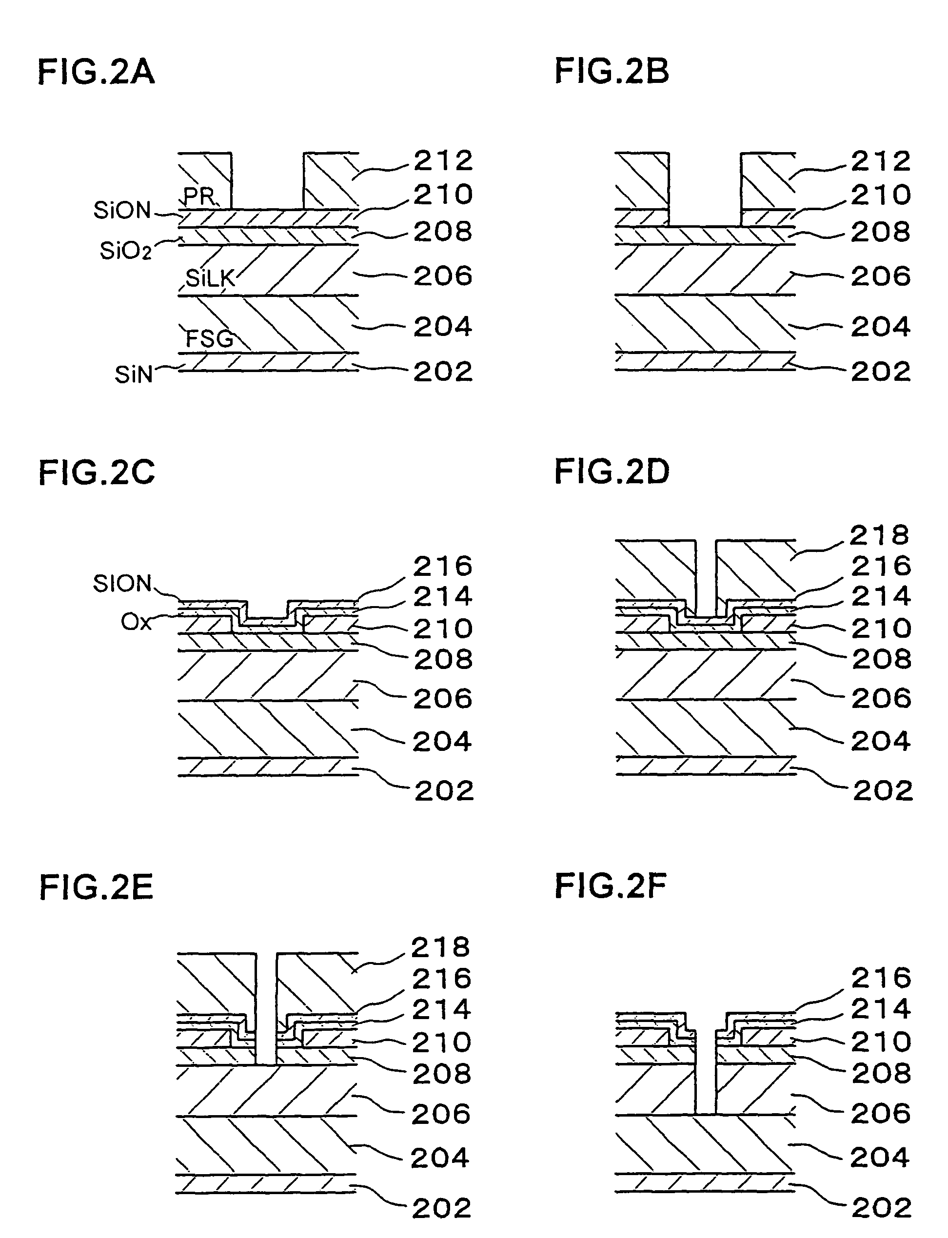
[0037]Next, the steps executed to form a dual damascene structure in the present invention by using the etching apparatus described above are explained in reference to FIGS. 2 and 3. As shown and FIG. 2A, an FSG layer 204 constituted of an inorganic low-k film (with a film thickness of 500 nm) is formed as a layer insulating film on top of an SiN layer 202 (with a film thickness of 50 nm), which functions as a protective film. Over the FSG layer 204, a SiLK™ layer 206 (with a film thickness of 400 nm) is formed as an organic low-k film. Over the SiLK™ layer 206, an SiO2 layer 208 (with a film thickness of 100 nm) constituting a first hard mask and an SiON layer 210 (with a film thickness of 100 nm) constituting a second hard mask are formed as hard mask layers to be used to form trenches and vias and, over the hard mask layers, a photoresist (PR) layer 212 having a pattern to be used for the trench formation is formed.
[0038]First, as shown in FIG. 2B, the SiON layer 210 constituting th
second embodiment
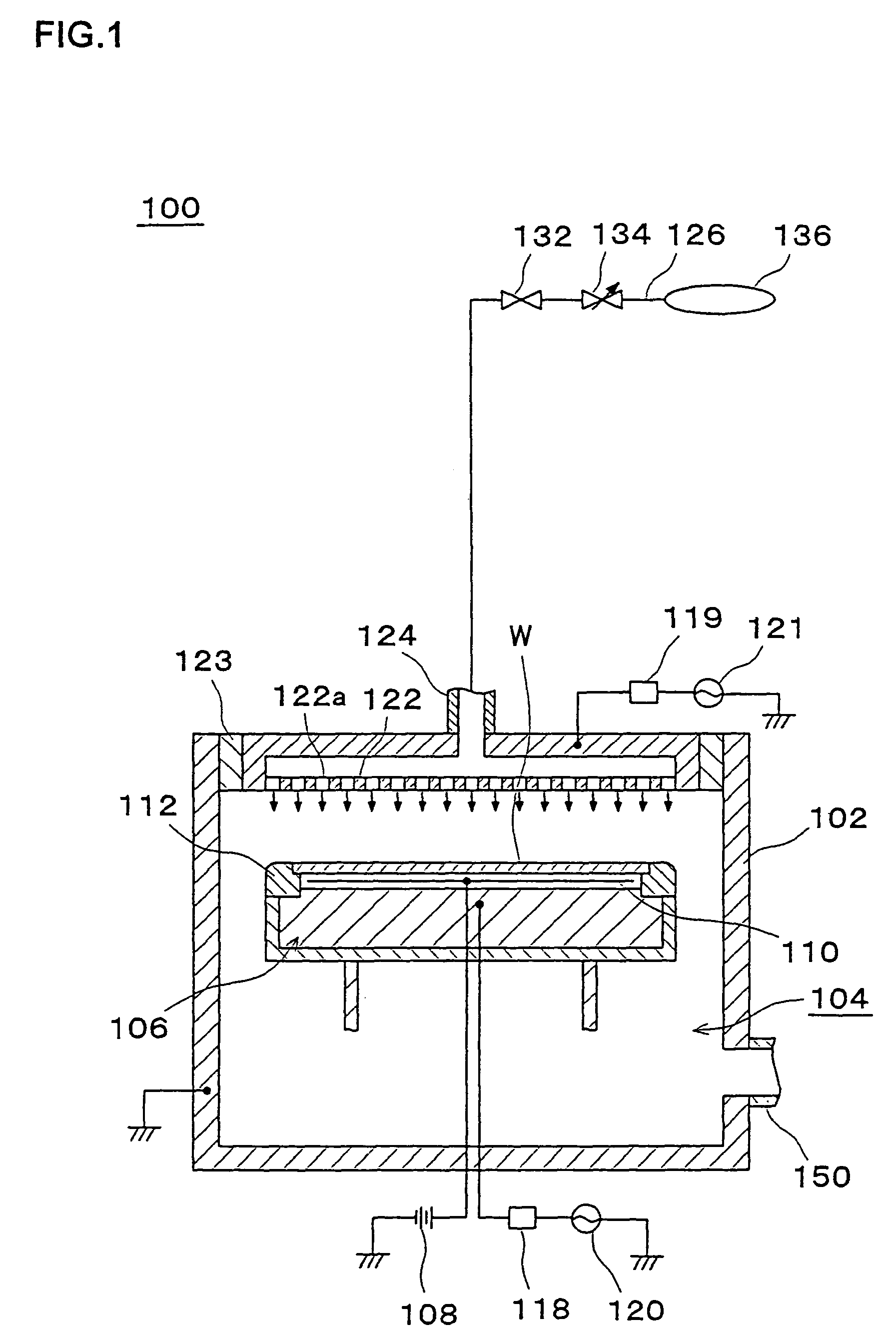
[0049]The following is an explanation of the steps executed to form a dual damascene structure in the present invention by using the etching apparatus shown in FIG. 1, given in reference to FIGS. 4 and 5. As shown in FIG. 4A, an FSG layer 204 is formed as an inorganic low-k film (with a film thickness of 500 nm) constituted of a layer insulating film on top of an SiN layer 202 (with a film thickness of 50 nm) as a protective film. Over the FSG layer 204, a SiLK™ layer 206 (with a film thickness of 400 nm) is formed as an organic low-k film. Over the SiLK™ layer 206, an SiON layer 308 (with a film thickness of 200 nm) constituting a first hard mask is formed as a hard mask layer to be used to form trenches and vias and, over the hard mask layers, a photoresist (PR) layer 212 having a pattern to be used for trench formation is formed.
[0050]First, as shown in FIG. 4B, the SiON layer 308 constituting the first hard mask is partially etched and a trench pattern is formed through a specific
PUM
 Abstract
Description
Claims
Application Information
 - R&D Engineer
- R&D Manager
- IP Professional
- Industry Leading Data Capabilities
- Powerful AI technology
- Patent DNA Extraction
Browse by: Latest US Patents, China's latest patents, Technical Efficacy Thesaurus, Application Domain, Technology Topic.
© 2024 PatSnap. All rights reserved.Legal|Privacy policy|Modern Slavery Act Transparency Statement|Sitemap