Semiconductor structure and method for manufacturing the same

a technology of semiconductors and semiconductors, applied in the direction of semiconductor devices, electrical equipment, transistors, etc., can solve the problems of inability to deal with the common provision of different types of devices, damage to low-voltage devices, and inability to generally function effectively at low-voltage devices

Active Publication Date: 2017-01-24
VANGUARD INTERNATIONAL SEMICONDUCTOR CORPORATION
View PDF8 Cites 0 Cited by
  • Summary
  • Abstract
  • Description
  • Claims
  • Application Information

AI Technical Summary

Benefits of technology

This patent describes a new design for an electronic component called a High Voltage Metal Oxide Semiconductor (HVMOS) device that improves its performance by reducing leak current and maintaining good electrical contact with other components.

Problems solved by technology

This patent describes a problem that arises when trying to integrate multiple electronic components on a single chip without sacrificing their performance. Existing methods require expensive processes and structures that may damage sensitive parts during operation. Therefore, there is a need for a more efficient method of integrating multiple electronic components onto a single chip without compromising its performance.

Method used


Image

  • Semiconductor structure and method for manufacturing the same
  • Semiconductor structure and method for manufacturing the same
  • Semiconductor structure and method for manufacturing the same

Examples


Embodiment Construction

[0014]The following description is of the best-contemplated mode of carrying out the disclosure. This description is made for the purpose of illustrating the general principles of the disclosure and should not be taken in a limiting sense. The scope of the disclosure is best determined by reference to the appended claims.

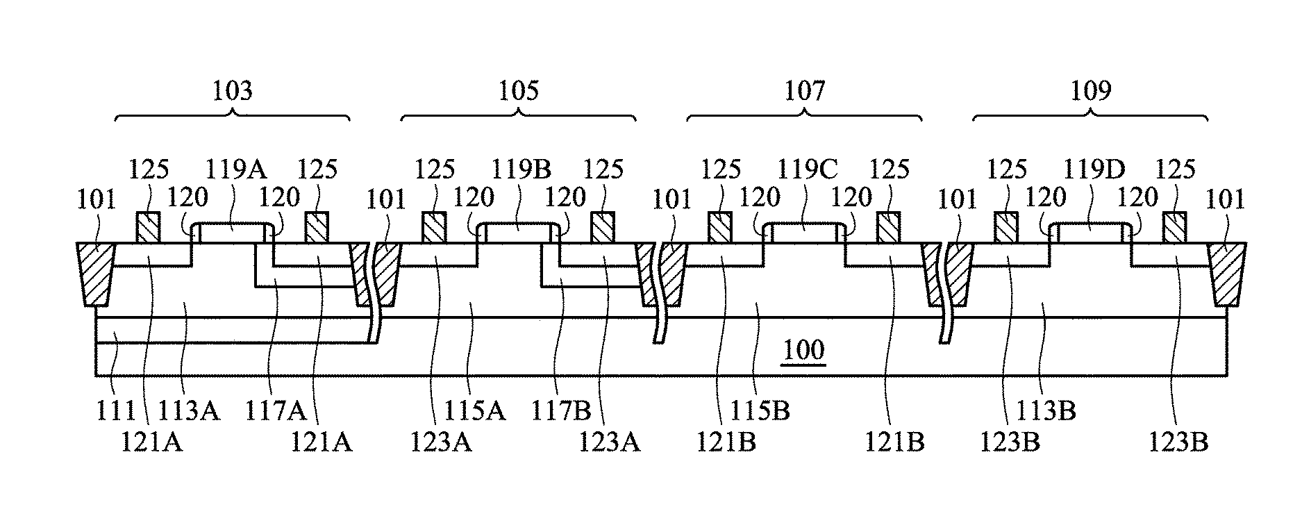
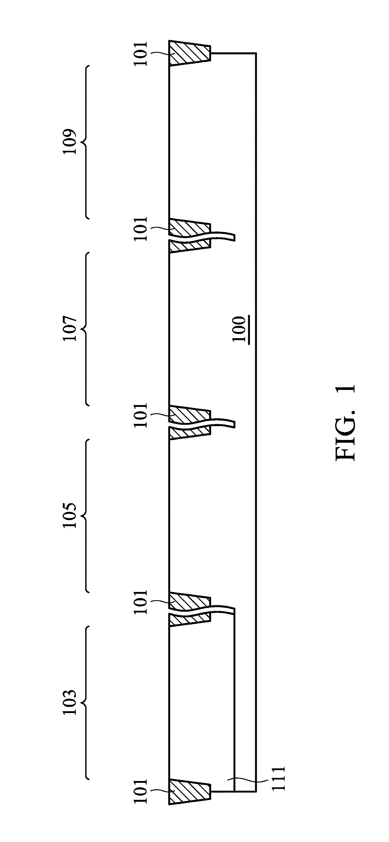
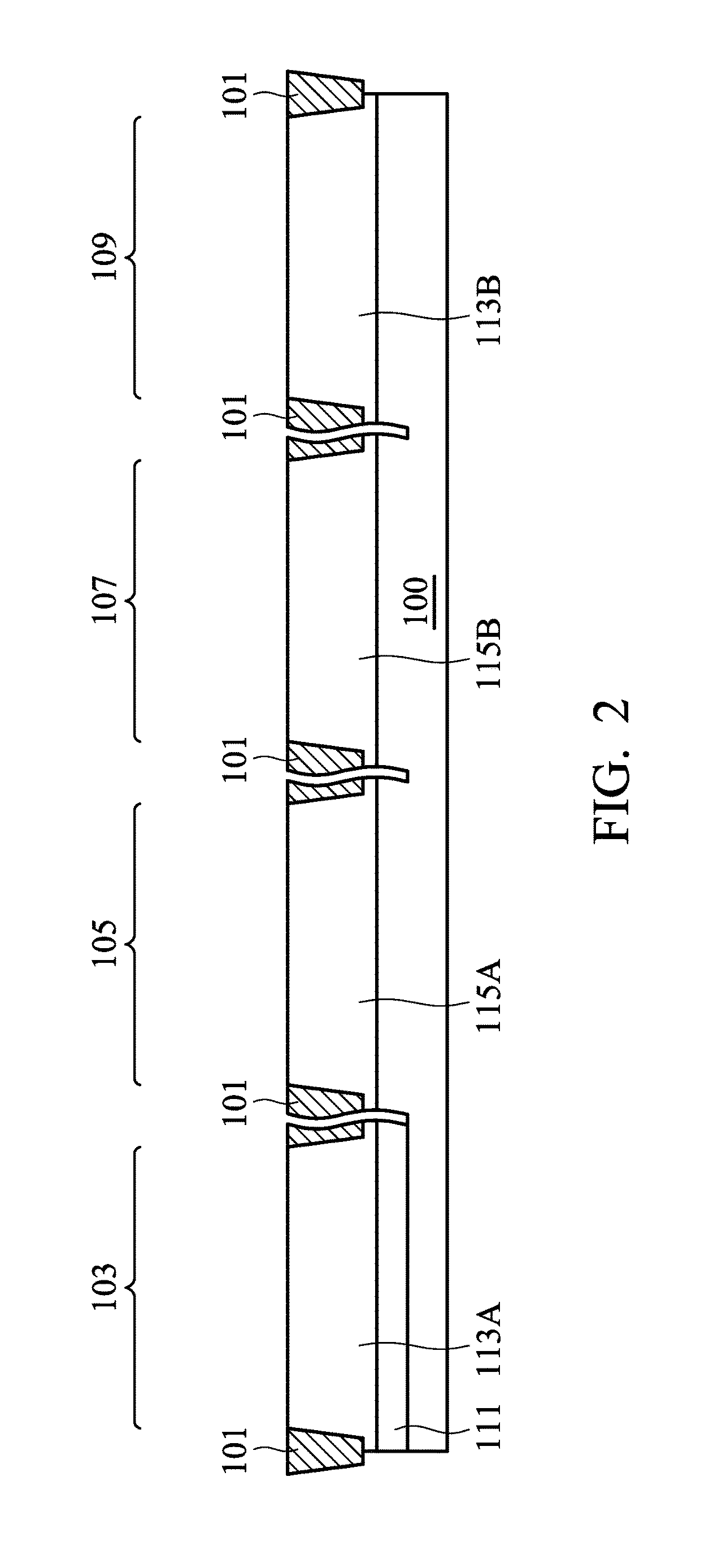
[0015]FIGS. 1 to 5 are cross sections of a semiconductor structure during manufacture in one embodiment. As shown in FIG. 1, a p-type substrate 100 is provided. The substrate 100 can be silicon substrate, a silicon-on-insulator (SOI) substrate, or the like. In one embodiment, a substrate 100 is provided, and then implanted by p-type dopants. Alternatively, the substrate 100 is formed by epitaxy growth and in-situ doped by the p-type dopants. In one embodiment, the substrate 100 has a doping concentration of 7e13 atoms / cm3 to 7e15 atoms / cm3.

[0016]Isolation structures 101 are then formed on the substrate 100 to separate and define a plurality of device regions, e.g.


PUM


Abstract

A semiconductor structure is provided, which includes a first high-voltage MOS device region having a first well and a first light-doping region in a part of the first well, wherein the conductive type of the first well and the conductive type of the first light-doping region are opposite. The first high-voltage MOS device region also includes a first gate stack on a part of the first well and a part of the first light-doping region, and first heavy-doping regions in the first well and the first light-doping region at two sides of the gate stack, wherein the conductive type of the first heavy-doping region and the conductive type of the first well are the same. The first light-doping region between the first well and the first heavy-doping regions is a channel region of the first high-voltage MOS device region.

Description


Claims


Application Information

Patent Timeline
Owner VANGUARD INTERNATIONAL SEMICONDUCTOR CORPORATION
Why Eureka
Try Eureka