Method for forming amorphous silicon oxide laminated structure

A technology of silicon oxide and stacked structure, which is applied in the direction of electrical components, semiconductor/solid-state device manufacturing, circuits, etc., can solve the problems of high time consumption, impact on production capacity, and low deposition rate, so as to reduce time consumption and increase production capacity Effect

Inactive Publication Date: 2011-05-25
SEMICON MFG INT (SHANGHAI) CORP +1
View PDF1 Cites 0 Cited by
  • Summary
  • Abstract
  • Description
  • Claims
  • Application Information

AI Technical Summary

Benefits of technology

The present technology improves upon previous methods for forming layers on semiconductor devices such as transistors or solar cells that use crystalline materials like monocrystal silane (SiH 4 ). By integrating these two types of material together during this manufacturing step, it can be done more efficiently than previously possible without sacrificing quality control over each other's properties. This results in improved performance and increased productivity.

Problems solved by technology

This patented describes methods for making high density solid state memories that have greater capacities than current types of RAM due to their ability to achieve more compact structures without compromising data integrity or reliability. These techniques include various ways like adding extra components called bit lines or providing space within certain areas where there may still exist empty spaces around them. Additionally, these processes involve growing multilevel materials at once instead of separately producing individual elements individually. Overall, this new approach allows for higher levels of integrated circuit functionality while maintaining precise dimensions and improved productivity compared to previous approaches.

Method used


Image

  • Method for forming amorphous silicon oxide laminated structure
  • Method for forming amorphous silicon oxide laminated structure
  • Method for forming amorphous silicon oxide laminated structure

Examples


Embodiment Construction

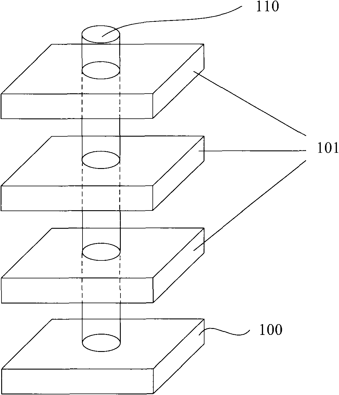
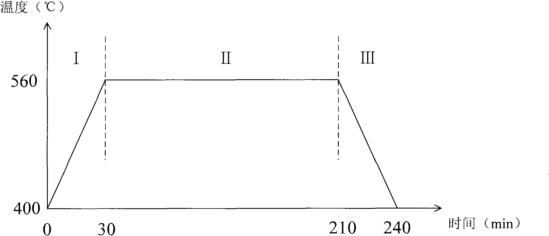
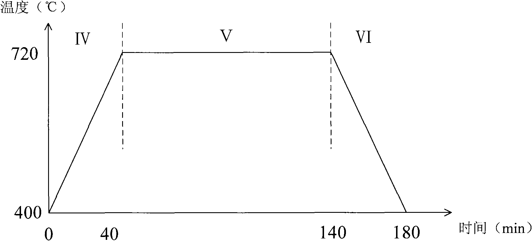
[0031] In the prior art, the reactant used in the deposition process of the amorphous silicon layer is silane, and the reaction temperature is about 560°C; while the reactant used in the deposition process of the silicon oxide layer is silane and nitrogen oxide, and the reaction temperature is about 720°C. The reaction temperature is different, so the amorphous silicon layer and the silicon oxide layer are respectively carried out in different deposition equipment. The semiconductor substrate is repeatedly transferred between two deposition equipments, on which layers of amorphous silicon and silicon oxide are alternately formed.

[0032] figure 2 and image 3 The relationship between the temperature and time of the semiconductor substrate during the formation of the amorphous silicon layer and the silicon oxide layer is given respectively. Such as figure 2 As shown, the formation process of the amorphous silicon layer is mainly divided into three stages: stage I, stage II a


PUM


Abstract

The invention discloses a method for forming an amorphous silicon oxide laminated structure, which comprises the steps of forming a silicon oxide layer by using chemical vapor deposition, wherein the reactants comprise chlorosilane and oxygen free radicals. The method reduces the reaction temperature of the amorphous silicon layer forming process, avoids repeated heating and cooling processes in the reaction process, reduces time consumption and improves the capacity.

Description


Claims


Application Information

Patent Timeline
Owner SEMICON MFG INT (SHANGHAI) CORP
Why Eureka
Try Eureka