Pixel unit read-out circuit and method, and pixel array read-out circuit and method
A pixel unit and readout circuit technology, which is applied in circuits, TVs, color TVs, etc., can solve the problems of complex readout circuit structure and timing, high power consumption of image sensor chips, and low fill factor, so as to reduce complexity and Circuit area, simple structure, effect of improving fill factor
- Summary
- Abstract
- Description
- Claims
- Application Information
AI Technical Summary
Problems solved by technology
Method used
Image

Examples
Example Embodiment
[0067] Example one
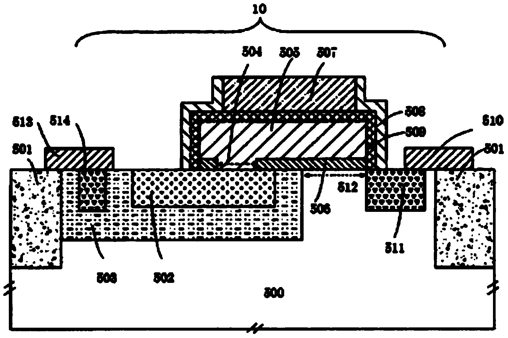
[0068] This embodiment provides a pixel unit readout circuit, which is suitable for connecting the output terminal of the pixel unit 100 to read out the readout signal of the pixel unit. Preferably, the pixel unit includes a half-floating gate transistor, a photodiode is included between the drain and the half-floating gate of the half-floating gate transistor, and the source of the half-floating gate transistor is the output terminal of the pixel unit.
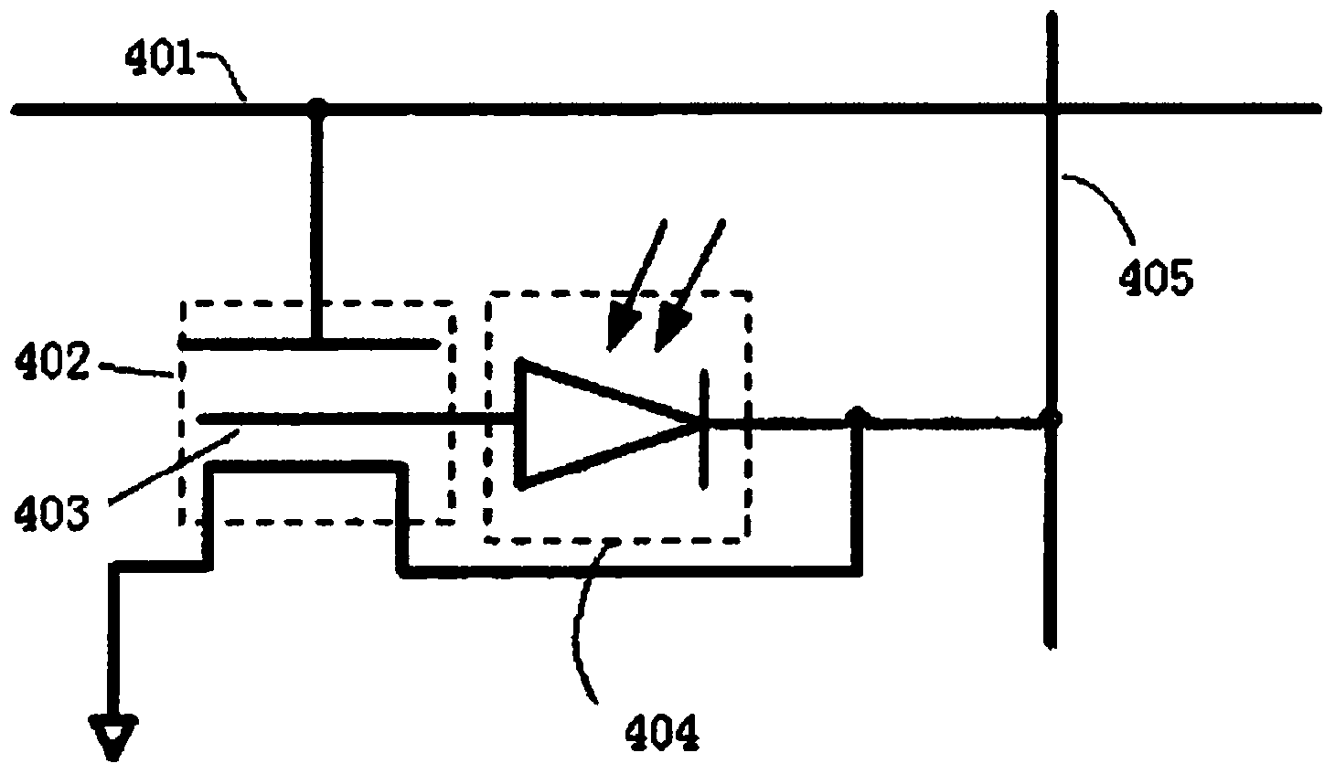
[0069] Such as Figure 5 As shown, the pixel unit readout circuit provided in this embodiment specifically includes: a voltage providing unit 200, a current comparing unit 300, and a counting unit 400. The output terminal of the pixel unit 100 and the output terminal of the voltage supply unit 200 are respectively connected to two input terminals of the current comparing unit 300, and the output terminal of the current comparing unit 300 is connected to the counting unit 400. The enable terminal EN is connected.
Example Embodiment
[0084] Example two
[0085] This embodiment provides a pixel array readout circuit.
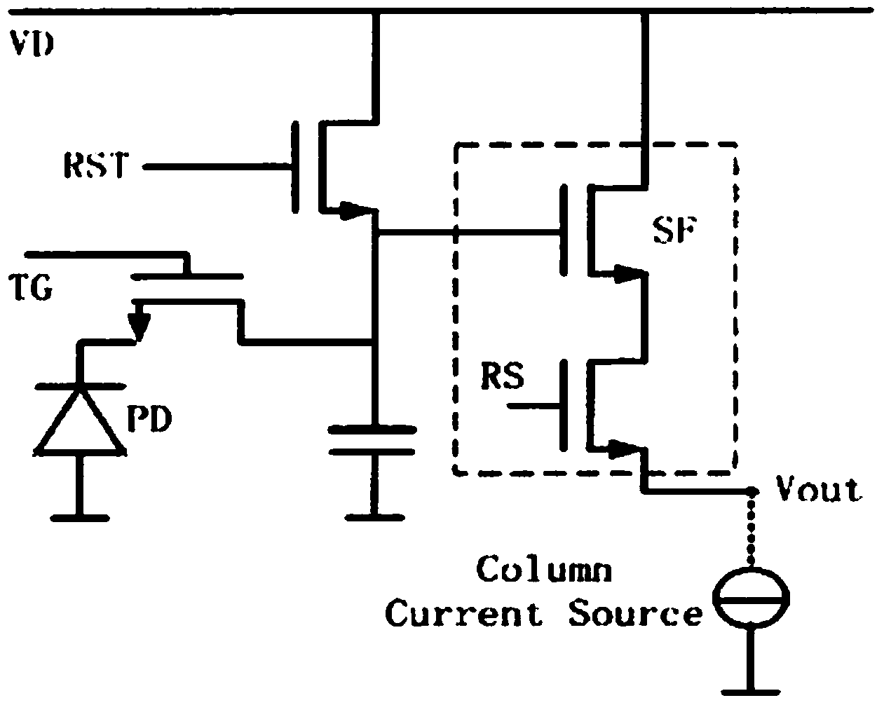
[0086] The pixel array is as Figure 4 The array structure shown includes at least one column of pixel units 100. Each pixel unit 100 includes half of floating gate transistors. The sources of the half floating gate transistors in the pixel units in each column are connected to each other and serve as the output of each column of pixel units. end.
[0087] Continue to refer Figure 5 As shown, specifically, the pixel array readout circuit provided by this embodiment includes: a voltage providing unit 200, a current comparing unit 300, and a counting unit 400; the output terminal of each column of pixel unit 100, an output of the voltage providing unit 200 The terminals are respectively connected to two input terminals of the current comparison unit 300, and the output terminal of the current comparison unit 300 is connected to the enable terminal EN of the counting unit 400.
[0088] The voltage supply
Example Embodiment
[0107] Example three
[0108] This embodiment provides a pixel array readout circuit, and the pixel array in this embodiment is similar to the second embodiment.
[0109] Continue to refer Figure 5 As shown, the pixel array readout circuit provided by this embodiment includes: a voltage providing unit 200, a current comparing unit 300, and a counting unit 400. The output terminal of each column of pixel units 100 and the output terminal of the voltage supply unit 200 are respectively connected to the two input terminals of the current comparing unit 300, and the output terminal of the current comparing unit 300 is connected to the output terminal of the counting unit 400. The enable terminal EN is connected.
[0110] Specific as Picture 9 As shown, the pixel array readout circuit provided in this embodiment is different from the second embodiment in that, assuming that the pixel array has n columns of pixels, the pixel array readout circuit provided in this embodiment includes: a cur
PUM
 Abstract
Description
Claims
Application Information
 - R&D Engineer
- R&D Manager
- IP Professional
- Industry Leading Data Capabilities
- Powerful AI technology
- Patent DNA Extraction
Browse by: Latest US Patents, China's latest patents, Technical Efficacy Thesaurus, Application Domain, Technology Topic.
© 2024 PatSnap. All rights reserved.Legal|Privacy policy|Modern Slavery Act Transparency Statement|Sitemap