Cascoded semiconductor devices

A cascading, transistor technology, applied in semiconductor devices, semiconductor/solid-state device components, electric solid-state devices, etc., can solve problems such as power supply short-circuit, GaN switches cannot operate reliably in reverse conduction mode, and achieve low switching losses. Effect

Active Publication Date: 2014-10-15
NEXPERIA BV
View PDF4 Cites 8 Cited by
  • Summary
  • Abstract
  • Description
  • Claims
  • Application Information

AI Technical Summary

Benefits of technology

In this invention it allows for efficient reversal on certain types of circuits called cascades that are designed with special features like rotating or free-winding functions. These circuitry allow for smooth movement without any loss during normal use.

Problems solved by technology

Technologies described in this patented technical problem addressed in these patent include improving the efficiency of switching elements like insulating gate type transists (IGSFTs)/silic germanium (SG)) based integrated circuits without causing excess energy consumption during operation due to large backward voltages generated by inverse polarity charges caused by external sources. Additionally, reducing resistance values associated with certain types of transistes reduces leakage current and allows more efficient use of space within electronic components.

Method used


Image

  • Cascoded semiconductor devices
  • Cascoded semiconductor devices
  • Cascoded semiconductor devices

Examples


Embodiment Construction

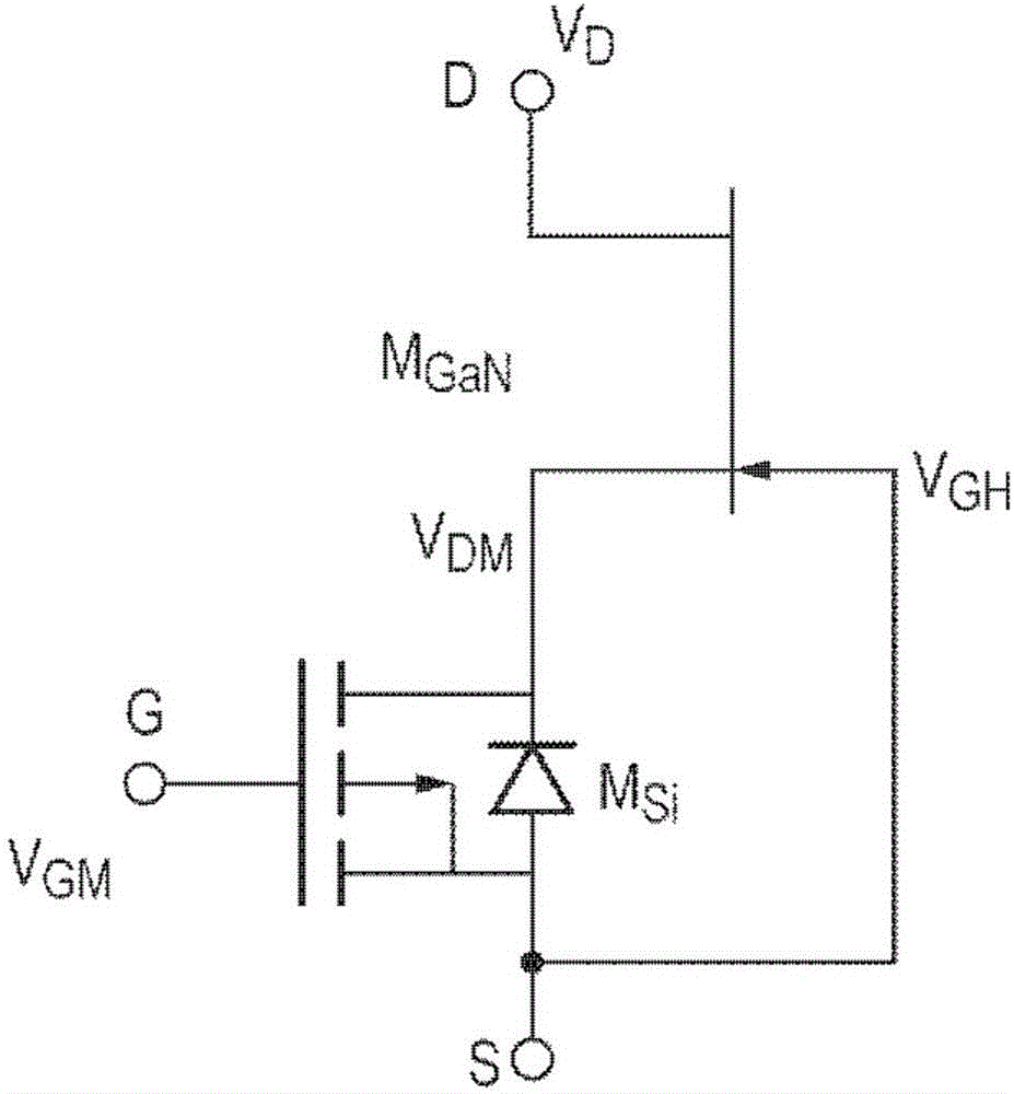
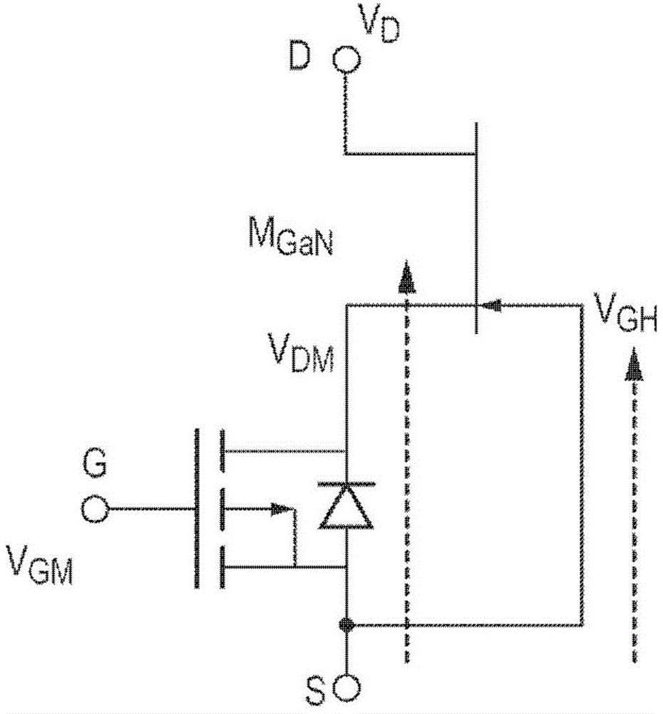
[0033] Embodiments of the present invention propose a cascode transistor circuit having a main depletion mode transistor and a cascode MOSFET formed, the two transistors being packaged to form the cascode transistor circuit. The bias circuit is connected between the gate of the power transistor and the low supply line of the circuit. A biasing circuit is integrated into the transistor circuit for compensating the forward voltage of the body diode of the cascaded MOSFET. In the absence of a bias circuit, the Schottky gate is in parallel with the body diode of the cascode MOSFET. Because the forward voltages can be nearly equal, a larger current can flow through the Schottky gate.

[0034] The bias circuit intentionally increases the forward voltage of the Schottky gate for reverse current, so all the current will flow through the MOSFET body diode.

[0035] Therefore, the proposed cascode transistor circuit structure can enable reliable reverse operation of the cascode switch.


PUM


Abstract

The invention provides a cascode transistor circuit with a depletion mode transistor and a switching device. A gate bias circuit is connected between the gate of the depletion mode transistor and the low power line. The gate bias circuit is adapted to compensate the forward voltage of a diode function of the switching device. The depletion mode transistor and the gate bias circuit are formed as part of an integrated circuit.

Description


Claims


Application Information

Patent Timeline
Owner NEXPERIA BV
Why Eureka
Try Eureka