Semiconductor device and manufacturing method thereof
A manufacturing method and semiconductor technology, applied in semiconductor/solid-state device manufacturing, semiconductor devices, electric solid-state devices, etc., can solve problems such as increased threshold voltage and reduced readout current, and achieve the effect of improving performance
- Summary
- Abstract
- Description
- Claims
- Application Information
AI Technical Summary
Benefits of technology
Problems solved by technology
Method used
Image

Examples
no. 1 example
[0053]
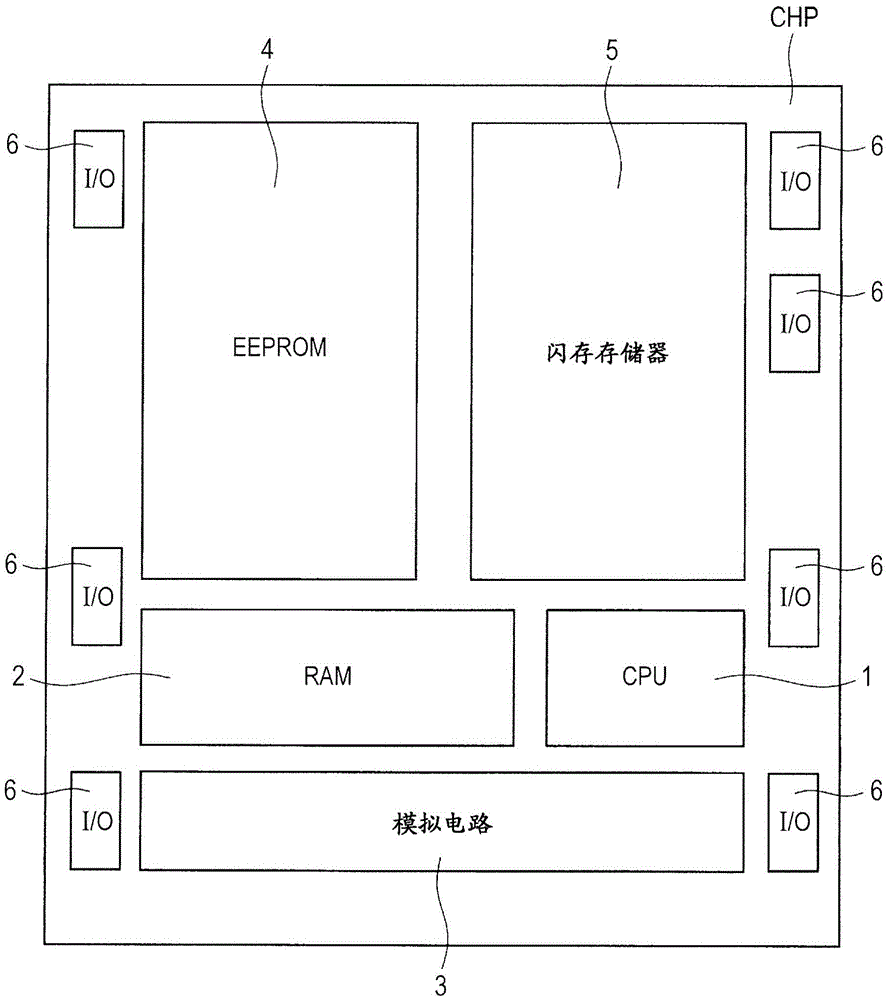
[0054] A semiconductor device having a nonvolatile memory in a first embodiment will be described with reference to the drawings. A layout configuration of a semiconductor device (semiconductor chip) in which a system including a nonvolatile memory is formed will be described first. figure 1 is a view showing an example of the layout configuration of the semiconductor chip CHP in the first embodiment. The semiconductor chip CHP has a CPU (Central Processing Unit) 1, RAM (Random Access Memory) 2, analog circuits 3, EEPROM (Electrically Erasable Programmable Read Only Memory) 4, flash memory 5, and I / O (Input / Output ) Circuit 6.
[0055] The CPU (circuit) 1 is also called a central processing unit, and corresponds to a core of a computer or the like. The CPU 1 reads out commands from the storage device to decode the commands, and executes various operations and controls based on the commands.
[0056] The RAM (circuit) 2 is a memory from which stored information
no. 2 example
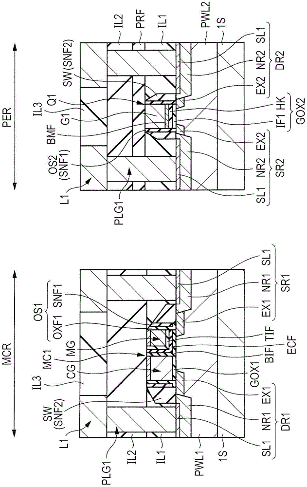
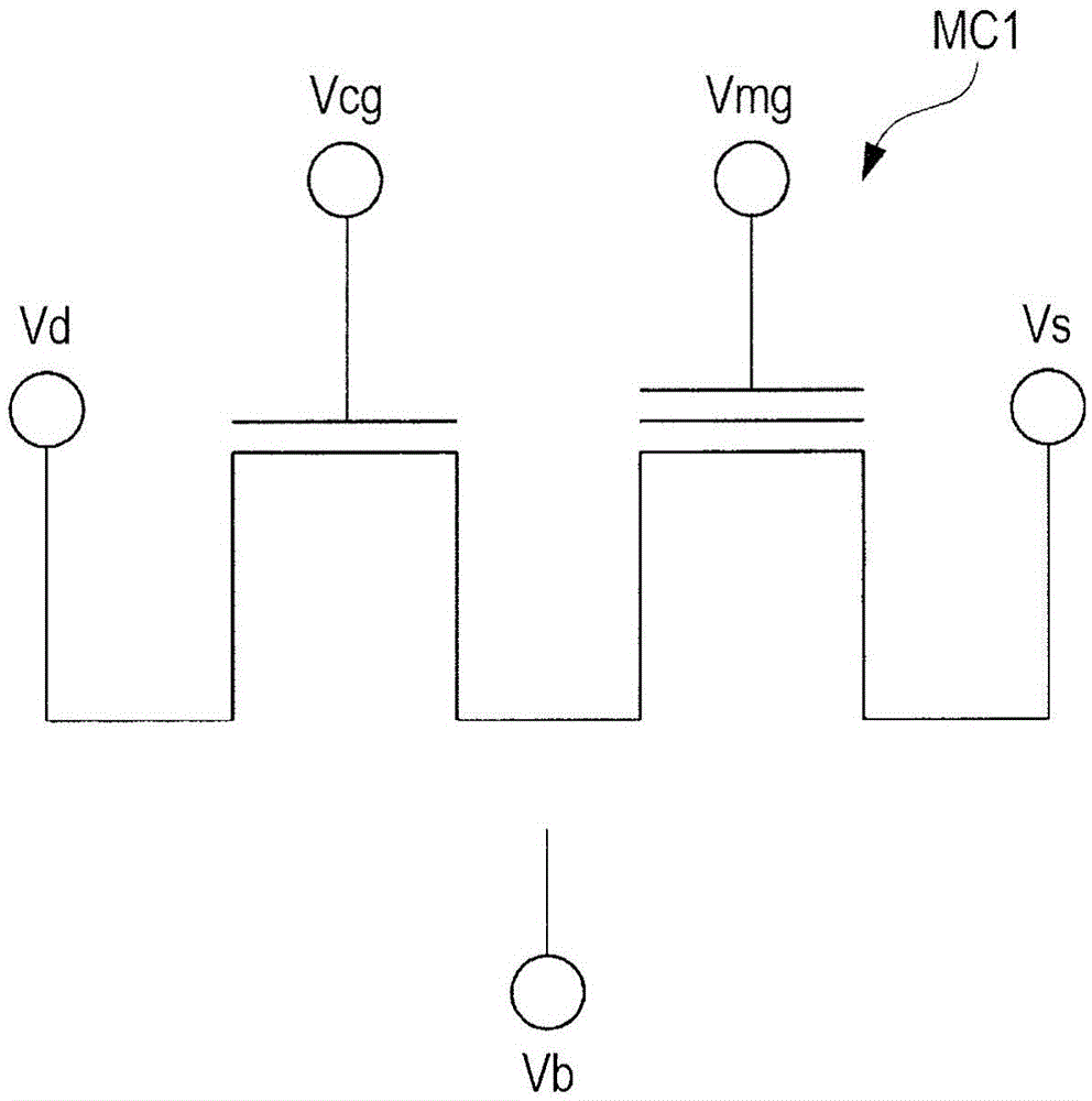
[0143] In the foregoing first embodiment, the silicon oxide film OXF1 is first formed in the memory cell formation region MCR, and then the silicon nitride film SNF1 is formed in the peripheral circuit formation region PER. Thus, in the first embodiment, the offset spacer in the memory cell MC1 is formed of both the silicon oxide film OXF1 in direct contact with the charge storage film ECF and the silicon nitride film SNF1 positioned over the silicon oxide film OXF1 OS1, and the offset spacer OS2 in the MISFET Q1 is formed from the silicon nitride film SNF1. On the other hand, an example will be described in the second embodiment in which the silicon nitride film SNF1 is first formed in the peripheral circuit formation region PER and then the silicon oxide film OXF1 is formed in the memory cell formation region MCR.
[0144]
[0145] After the dummy gate electrode DG1 is formed in the peripheral circuit formation region PER, a silicon nitride film SNF1 is formed over the semico
no. 3 example
[0153]
[0154] (Back Gate + Back HK)
[0155] Since the manufacturing method of the semiconductor device in the third embodiment is almost the same as that of the first embodiment, description will be made focusing on different points.
[0156] A dummy gate electrode DG1 and an insulating film IF1 including, for example, a silicon oxide film (see Figure 22 ).
[0157] Subsequently, a silicon oxide film OXF1 is formed over the semiconductor substrate 1S, and then is left only in the memory cell formation region MCR by photolithography and wet etching, thereby covering the control gate electrode CG and the memory gate electrode CG. The silicon oxide film OXF1 of the electrode MG is formed (see Figure 23 ). At this time, the silicon oxide film OXF1 formed in the peripheral circuit formation region PER is removed.
[0158] Subsequently, after the silicon nitride film SNF1 is formed over the semiconductor substrate 1S, the silicon nitride film SNF1 is etched back by anisotrop
PUM
 Abstract
Description
Claims
Application Information
 - R&D Engineer
- R&D Manager
- IP Professional
- Industry Leading Data Capabilities
- Powerful AI technology
- Patent DNA Extraction
Browse by: Latest US Patents, China's latest patents, Technical Efficacy Thesaurus, Application Domain, Technology Topic.
© 2024 PatSnap. All rights reserved.Legal|Privacy policy|Modern Slavery Act Transparency Statement|Sitemap