Array substrate row drive circuit and drive method thereof

A technology of array substrate row and drive circuit, applied in instruments, static indicators, etc., can solve problems such as affecting the potential of Q point, abnormal panel display, abnormal output waveform, etc., and achieve the effect of avoiding overlapping in time

Active Publication Date: 2017-05-31
SHENZHEN CHINA STAR OPTOELECTRONICS TECH CO LTD
View PDF3 Cites 2 Cited by
  • Summary
  • Abstract
  • Description
  • Claims
  • Application Information

AI Technical Summary

Benefits of technology

This technology allows an LCD (Liquid Crystalline Display) screen to work properly even when it's exposed during extreme temperatures such as those found inside vehicles. It achieves this without adding extra components like temperature sensing devices or complicated circuits.

Problems solved by technology

This patented describes how current techniques for manufacturing LCD panels are affected by heating during production processes that can lead to issues like reduced performance or even damage to components within these devices.

Method used


Image

  • Array substrate row drive circuit and drive method thereof
  • Array substrate row drive circuit and drive method thereof
  • Array substrate row drive circuit and drive method thereof

Examples


no. 1 example

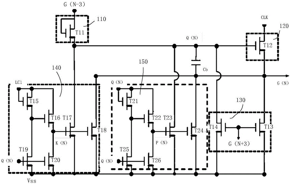
[0035] In the prior art, the input terminals of the array substrate row drive modules with a set number of stages receive the same pull-up control signal. Since there is a time overlap between the high potential signal output by the gate and the high potential of the pull-up control signal, the array substrate row drive circuit Under the environment of high temperature operation, the potential of the Q node will be affected, resulting in the abnormal output waveform of the set number of stages and the abnormal panel display.

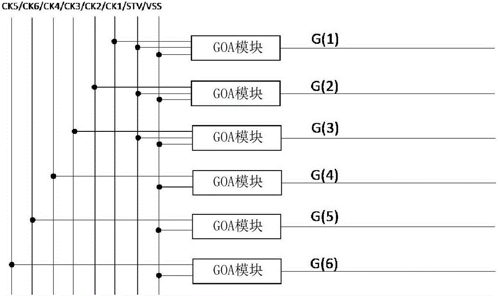
[0036] Based on this, this embodiment provides an array substrate row driving circuit, including: a multi-stage array substrate row driving module and a plurality of thin film transistors. Receive different pull-up control signals and output corresponding gate signals;

[0037] For each array substrate row driving module with a set number of stages, the falling edge of the pull-up control signal received at its input terminal is aligned with the rising edge

no. 2 example

[0051] Figure 7 It is a schematic diagram of the implementation flow of the driving method of the row driving circuit of the array substrate according to the second embodiment of the present invention. As shown in the figure, it may include the following steps:

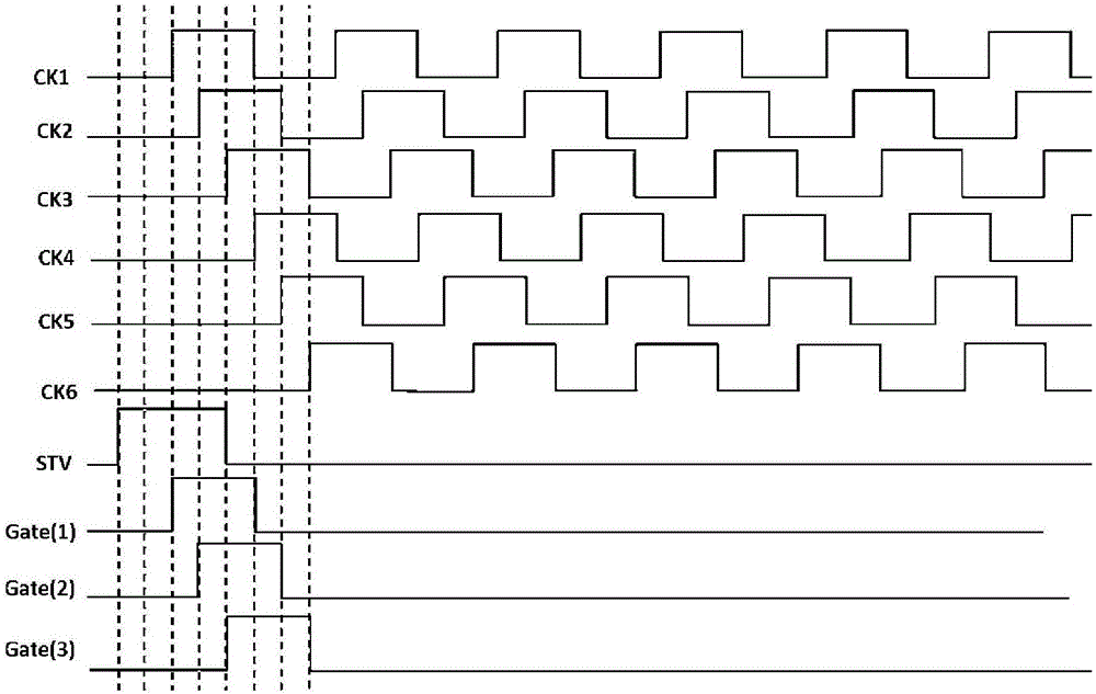
[0052] S710. Determine the different pull-up control signals corresponding to the array substrate row driving modules of the set number of stages. For each array substrate row driving module of the set number of stages, the falling edge of the corresponding pull-up control signal is connected The rising edge of the pole signal is aligned.

[0053] Taking the array substrate row driving modules with the set number of stages as the first two-stage array substrate row driving modules as an example, the first two-stage array substrate row driving modules include a first-stage array substrate row driver module and a second-stage array substrate row driver module. module, the first pull-up control signal corresponding to the


PUM


Abstract

The invention discloses an array substrate row drive circuit and a drive method of the array substrate row drive circuit. The array substrate row drive circuit comprises a plurality of levels of array substrate row drive modules and a plurality of thin film transistors, wherein the input ends of the array substrate row drive modules with the set level number receive different upwards pulling control signals through the corresponding thin film transistors and output corresponding grid signals; for each of the array substrate row drive modules with the set level number, the falling edge of the upwards pulling control signals received by the input end of the array substrate row drive module is level with the rising edge of the grid signals output by the input end of the array substrate row drive module. With the adoption of the scheme, the circuit and the method have the advantages that the overlapping in time of the upwards pulling control signals received by the input ends of the array substrate row drive modules with the set level number and the grid signals output by the input ends of the array substrate row drive modules with the set level number can be avoided, so that the Q node electric potential is not influenced when the array substrate row drive circuit is in the high-temperature operation environment, and then a liquid crystal display panel can be normally used in the high-temperature operation environment.

Description


Claims


Application Information

Patent Timeline
Owner SHENZHEN CHINA STAR OPTOELECTRONICS TECH CO LTD
Why Eureka
Try Eureka