Compound semiconductor silicon-based mixer device and preparation method thereof

A semiconductor and compound technology, applied in the field of compound semiconductor silicon-based hybrid devices and its preparation, can solve the problems of difficult alignment and complicated preparation process, and achieve the effects of improving efficiency, improving coupling efficiency, and improving integration

Pending Publication Date: 2018-05-18
SUZHOU JUZHEN PHOTOELECTRIC
View PDF7 Cites 5 Cited by
  • Summary
  • Abstract
  • Description
  • Claims
  • Application Information

AI Technical Summary

Benefits of technology

The present inventions provide methods for making high precision electronic components such as transistors or diodes without requiring expensive equipment like lasers. These techniques involve creation of specific structures called microstructures within the material used to make these materials. By aligning them correctly, they become more efficient when integrated into other parts of their own technology. Additionally, this technique allows for easier handling of different types of elements due to the lack of any physical contact between each element's surface and another part of the circuit board. Overall, it provides better quality products and increased productivity through reduced costs compared to traditional processes.

Problems solved by technology

This patented technical problem addressed by this patents relates to improving the performance and functionality of electronic systems such as computer chips while integrating both photoconversion elements and signal amplification functions into single units on their own substrate called Silicon Microcavity Integrated Circuits or SiC MICs. Current methods involve either aligning the lasers directly during assembly or attaching the lased wafers separately from the wafer used for signal amplifications. These techniques require precise placement but increase manufacturing costs associated therewith.

Method used


Image

  • Compound semiconductor silicon-based mixer device and preparation method thereof
  • Compound semiconductor silicon-based mixer device and preparation method thereof
  • Compound semiconductor silicon-based mixer device and preparation method thereof

Examples


Embodiment 1

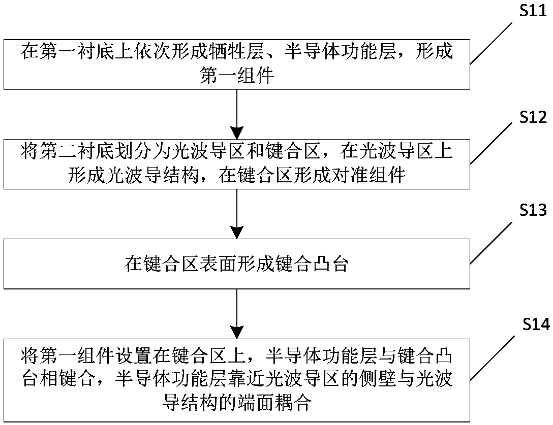
[0037] An embodiment of the present invention provides a method for preparing a compound semiconductor silicon-based hybrid device, which is used to prepare a silicon-based compound semiconductor hybrid integrated device, such as figure 1 Shown, this preparation method comprises the following steps:

[0038] Step S11 , sequentially forming a sacrificial layer and a semiconductor functional layer on the first substrate to form a first component.

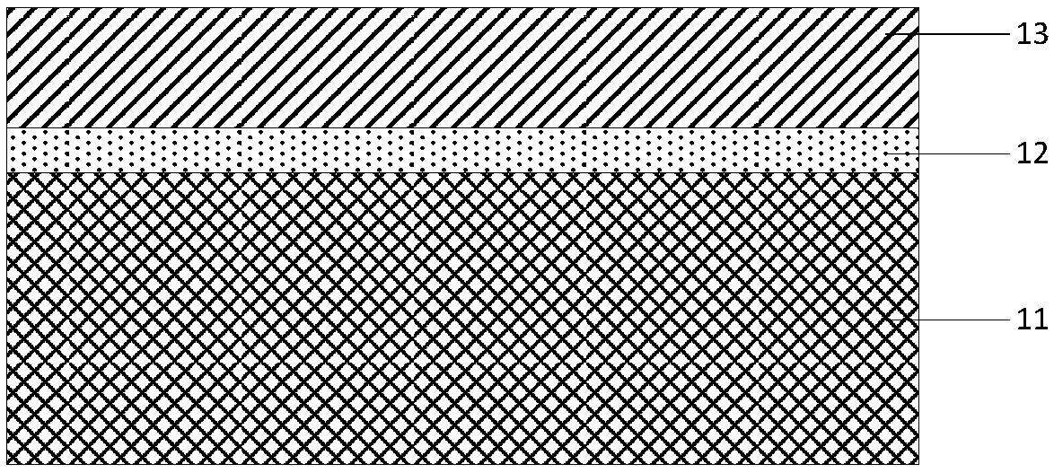
[0039] Such as figure 2 As shown, a sacrificial layer 12 is first grown on a first substrate 11 by molecular beam epitaxy (Molecular Beam Epitaxy, referred to as MBE) or metal-organic chemical vapor deposition (Metal-organic Chemical Vapor Deposition, referred to as MOCVD). A semiconductor functional layer (light gain and absorption structures such as semiconductor lasers, semiconductor optical amplifiers, and semiconductor photodetectors) 13 is grown on the layer 12 to form a first component. However, the protection scope of the pres

Embodiment 2

[0072] An embodiment of the present invention provides a silicon-based compound semiconductor hybrid integrated device, which is prepared by using the method for preparing a compound semiconductor silicon-based hybrid device in Embodiment 1 of the present invention.

[0073] For details of the structure of the compound semiconductor bulk silicon-based hybrid device not specifically described in this embodiment, please refer to Embodiment 1, and details will not be repeated here.


PUM

PropertyMeasurementUnit
Thicknessaaaaaaaaaa

Abstract

The invention relates to the technical field of semiconductors, and provides a compound semiconductor silicon-based mixer device and a preparation method thereof. The preparation method comprises thesteps of sequentially forming a sacrificial layer and a semiconductor function layer on a first substrate to form a first component, dividing a second substrate into an optical waveguide region and abonding region, forming an optical waveguide structure on the optical waveguide region, forming an alignment assembly in the bonding region, forming a bonding boss on the surface of the bonding region; arranging a first component on the bonding region, wherein the semiconductor function layer is bonded with the bonding boss, and the side wall, close to the optical waveguide region, of the semiconductor function layer is coupled with the end surface of the optical waveguide structure. According to the method, the problem of accurate alignment (namely passive alignment in the vertical directionand the horizontal direction) of the semiconductor function layer and the optical waveguide structure can be avoided. In addition, the integration degree of the semiconductor device and the coupling degree of the compound semiconductor photoelectric device and a silicon-based optical waveguide are improved, and the production efficiency is improved.

Description


Claims


Application Information

Patent Timeline
Owner SUZHOU JUZHEN PHOTOELECTRIC
Why Eureka
Try Eureka