A display device and a preparation method thereof

A technology for display devices and display areas, which is applied in semiconductor/solid-state device manufacturing, electrical components, electric solid-state devices, etc., can solve problems such as poor linearity, package failure, and edge overflow of organic layers, so as to improve edge linearity and increase Stability, the effect of promoting uniform diffusion

Inactive Publication Date: 2019-01-22
WUHAN CHINA STAR OPTOELECTRONICS SEMICON DISPLAY TECH CO LTD
View PDF6 Cites 17 Cited by
  • Summary
  • Abstract
  • Description
  • Claims
  • Application Information

AI Technical Summary

Benefits of technology

This patented technology allows for better control over how well an OLED material forms its own protective shell around tiny microscopes called pixels inside. By controllably injecting liquid into specific areas within these small spaces or create cavities where they form channels through which light travels effectively without being blocked up by other materials like metal layers. These technical improvements improve the performance and lifespan of electronic devices made therefrom while maintaining their quality level.

Problems solved by technology

The technical problem addressed by this patented solution is how to improve the performance of thin films made with these layers during manufacturing processes without causing damage or failures due to excessive flowability caused by previous methods such as solvent evaporation techniques.

Method used


Image

  • A display device and a preparation method thereof
  • A display device and a preparation method thereof
  • A display device and a preparation method thereof

Examples


Embodiment Construction

[0032] The following descriptions of the various embodiments refer to the accompanying drawings to illustrate specific embodiments in which the invention may be practiced. The directional terms mentioned in the present invention, such as [top], [bottom], [front], [back], [left], [right], [inside], [outside], [side], etc., are only for reference The orientation of the attached schema. Therefore, the directional terms used are used to illustrate and understand the present invention, but not to limit the present invention. In the figures, structurally similar elements are denoted by the same reference numerals.

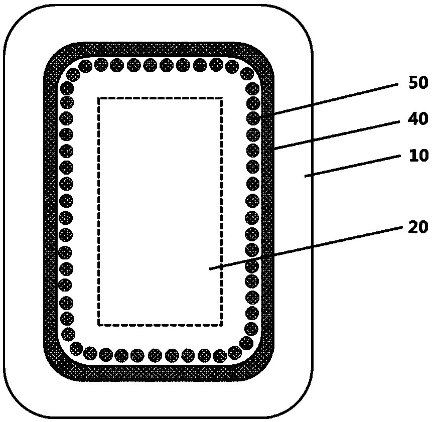
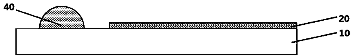
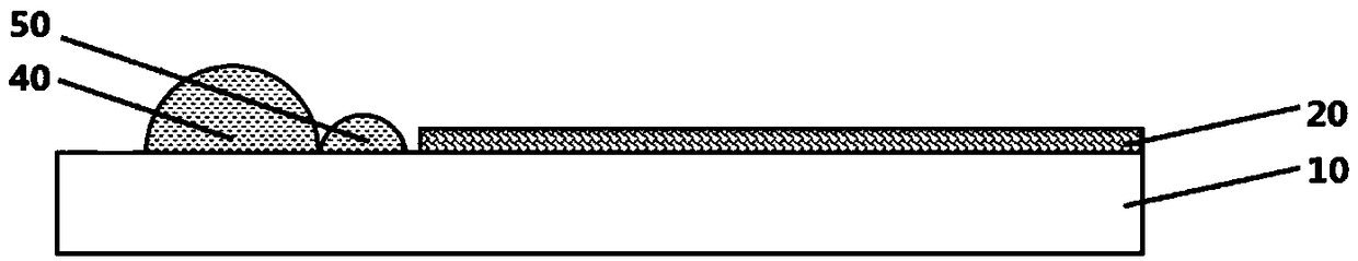
[0033] The present invention aims at the technical problem that the edge of the organic layer of the thin-film encapsulation layer "overflows" and "indents" in the display device of the prior art, and there is a risk of poor linearity of the organic layer, which eventually leads to encapsulation failure. This embodiment can solve this defect.

[0034] Such as figure 1 A


PUM

PropertyMeasurementUnit
Widthaaaaaaaaaa
Widthaaaaaaaaaa

Abstract

The invention provides a display device and a preparation method thereof. The display device comprises a display panel including a display area and a non-display area located at the periphery of the display area. A retaining wall prepared on the display panel around the display area; A thin film encapsulation layer prepared on the display panel and comprising an inorganic layer and an organic layer arranged in a stack; Wherein the retaining wall comprises a blocking part and a shunt part, wherein the blocking part surrounds the display area, the shunt part is located in an annular region formed by the boundary of the blocking part and the boundary of the display area, and the shunt part and the blocking part are combined to form a shunt passage for blocking and shunting the edge part of the organic layer.

Description


Claims


Application Information

Patent Timeline
Owner WUHAN CHINA STAR OPTOELECTRONICS SEMICON DISPLAY TECH CO LTD
Why Eureka
Try Eureka