Chip packaging structure and chip packaging method
A chip packaging structure and chip packaging technology, applied in the direction of electrical components, electric solid devices, circuits, etc., can solve the problems of increasing the original chip area, easy displacement of glue, and large packaging area, so as to reduce the probability of false soldering and prevent Effect of mechanical vibration and improvement of mechanical performance
- Summary
- Abstract
- Description
- Claims
- Application Information
AI Technical Summary
Problems solved by technology
Method used
Image

Examples
Example Embodiment
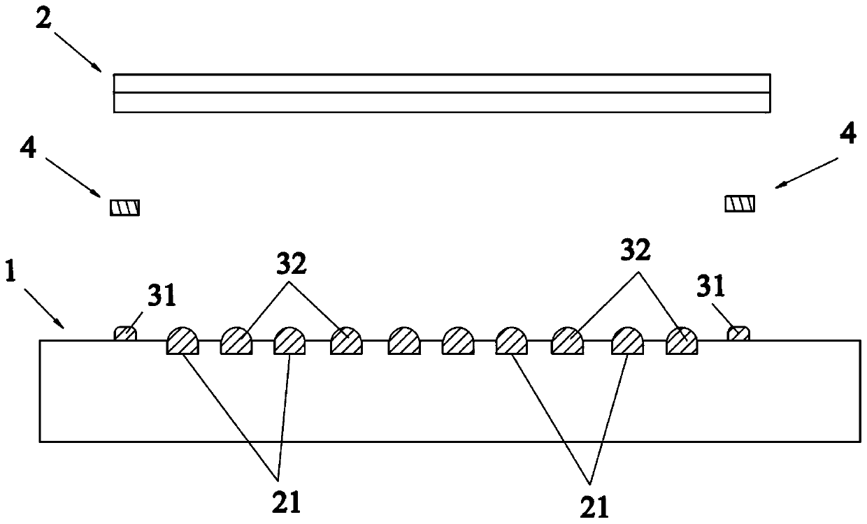
[0029] Example 1
[0030] Such as Figure 1~2 As shown, a chip packaging structure includes a circuit board 1 and an IC chip 2 mounted on the circuit board 1. A first solder paste 31 is provided on the surface of the circuit board 1, and the first solder paste 31 is provided around the IC chip 2 or It is arranged under the IC chip 2, a solid glue 4 is arranged on the first solder paste 31, and the solid glue 4 is used to bond the IC chip 2 to the circuit board 1. Before the IC chip 2 is bonded to the circuit board 1, the glue between the two is prone to displacement, which affects the chip packaging effect. Therefore, the first solder paste 31 is provided on the surface of the circuit board 1. A solid glue 4 is provided. The first solder paste 31 can be printed on the surface of the circuit board 1 by a printer and surround the surface of the circuit board 1 and the IC chip 2, or be arranged under the IC chip 2. The solid glue 4 is in progress. During reflow soldering, the heat me
Example Embodiment
[0040] Example 2
[0041] The difference from Embodiment 1 is that a part of the solid glue 4 in this embodiment extends to the inside or outside of the IC chip 2, the shape of the first solder paste 31 is a strip shape, and the shape of the solid glue 4 is a sheet shape. According to actual production requirements, the shape of the first solder paste 31 can be designed as a strip, and the contact area between the first solder paste 31 and the solid glue 4 can be increased to achieve a better fixing effect of the solid glue 4. The shape of the solid glue 4 It is designed in a sheet shape to increase the contact area between the first solder paste 31 and the solid glue 4 and improve the reliability between the two.
[0042] The other structure is the same as that of Embodiment 1, and will not be repeated here.
Example Embodiment
[0043] Example 3
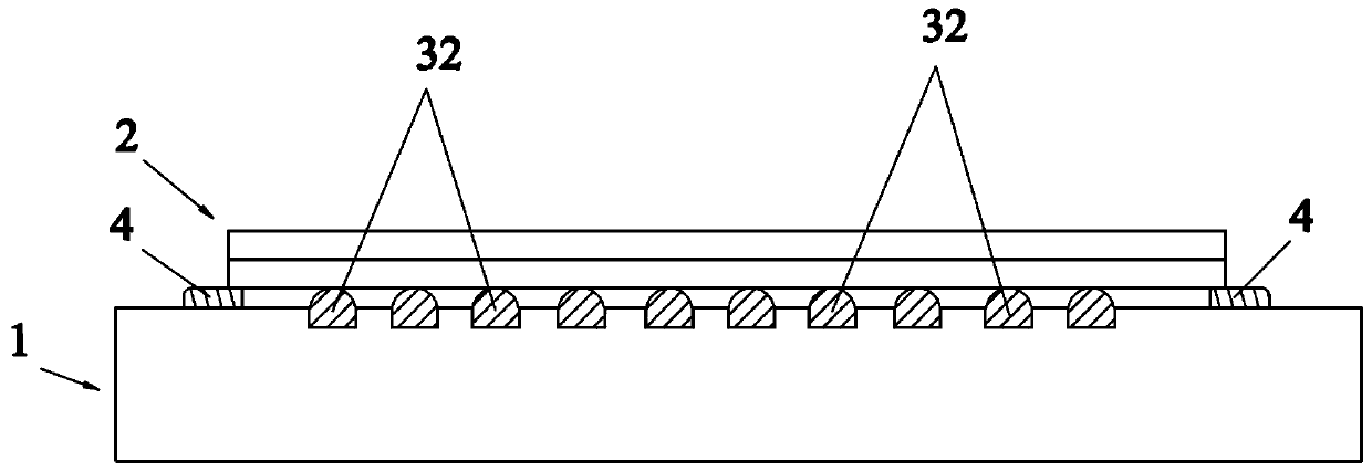
[0044] Such as Figure 1~2 As shown, a chip packaging method includes:
[0045] Printing the first solder paste 31 on the circuit board 1 so that the first solder paste 31 surrounds or under the IC chip 2;
[0046] Place the solid glue 4 on top of the first solder paste 31;
[0047] Through the reflow soldering, the solid glue 4 is heated to melt and solidify, so that a part of the solid glue 4 extends to the inside of the IC chip 2 and the other part of the solid glue 4 extends to the outside of the IC chip 2.
[0048] It should be noted that in the packaging method of the present invention, a printer is used to print the first solder paste 31 on the circuit board 1, and surround the surface of the circuit board 1 corresponding to the IC chip 2 or set it under the IC chip 2. A solder paste 31 can be printed in dots, and the first solder paste 31 is used to fix the solid glue 4; the strip-shaped solid glue 4 is fixed on the first solder paste 31 using a chip mounter, a
PUM
 Abstract
Description
Claims
Application Information
 - R&D Engineer
- R&D Manager
- IP Professional
- Industry Leading Data Capabilities
- Powerful AI technology
- Patent DNA Extraction
Browse by: Latest US Patents, China's latest patents, Technical Efficacy Thesaurus, Application Domain, Technology Topic.
© 2024 PatSnap. All rights reserved.Legal|Privacy policy|Modern Slavery Act Transparency Statement|Sitemap