Electrostatic protection structure and electrostatic protection circuit
An electrostatic protection and resistance technology, applied in circuits, electrical components, electric solid devices, etc., can solve problems such as poor electrostatic protection ability, and achieve the effect of improving conduction uniformity
- Summary
- Abstract
- Description
- Claims
- Application Information
AI Technical Summary
Benefits of technology
Problems solved by technology
Method used
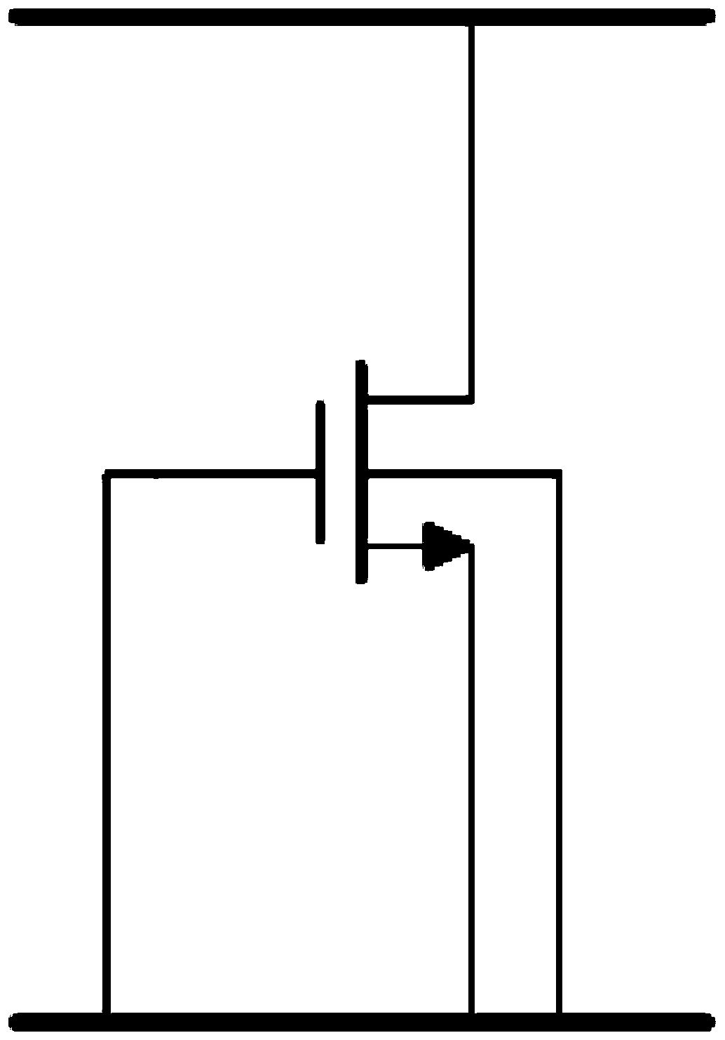
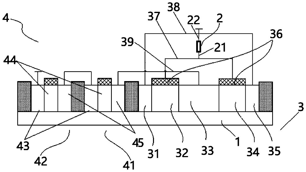
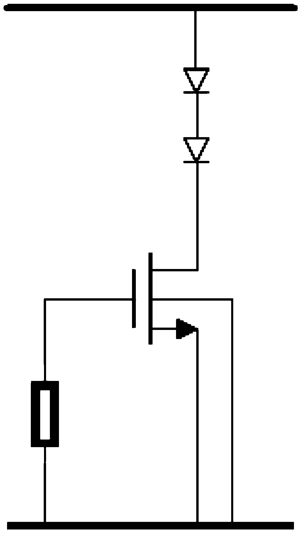
Image

Examples
Embodiment Construction
[0028] In order to make the purpose, technical solutions and advantages of the embodiments of the present application clearer, the embodiments of the present application will be further described in detail below in conjunction with the accompanying drawings. Apparently, the described embodiment is only an embodiment of the embodiments of the present application, but not all of the embodiments. Based on the embodiments of the present application, all other embodiments obtained by persons of ordinary skill in the art without creative efforts fall within the protection scope of the present invention.
[0029] It should be noted that the "embodiment" referred to here refers to a specific feature, structure or characteristic that may be included in at least one implementation manner of the embodiment of the present application. In the description of the embodiments of the present application, the terms "first", "second", "third" and "fourth" are used for descriptive purposes only, and
PUM
 Abstract
Description
Claims
Application Information
 - R&D Engineer
- R&D Manager
- IP Professional
- Industry Leading Data Capabilities
- Powerful AI technology
- Patent DNA Extraction
Browse by: Latest US Patents, China's latest patents, Technical Efficacy Thesaurus, Application Domain, Technology Topic.
© 2024 PatSnap. All rights reserved.Legal|Privacy policy|Modern Slavery Act Transparency Statement|Sitemap