Conductive nano foam and processing technology thereof
A conductive nano and conductive foam technology, which is applied to the conductive layer on the insulating carrier, the equipment and circuits used to manufacture the conductive/semi-conductive layer, etc., can solve the problem that the conductive foam does not have the heat dissipation function and the conductive performance of the conductive foam. Poor, ultra-thin products cannot be done, etc., to achieve the effect of good heat dissipation, barrier-free production and processing, and good elasticity
- Summary
- Abstract
- Description
- Claims
- Application Information
AI Technical Summary
Benefits of technology
Problems solved by technology
Method used
Image

Examples
Embodiment 1
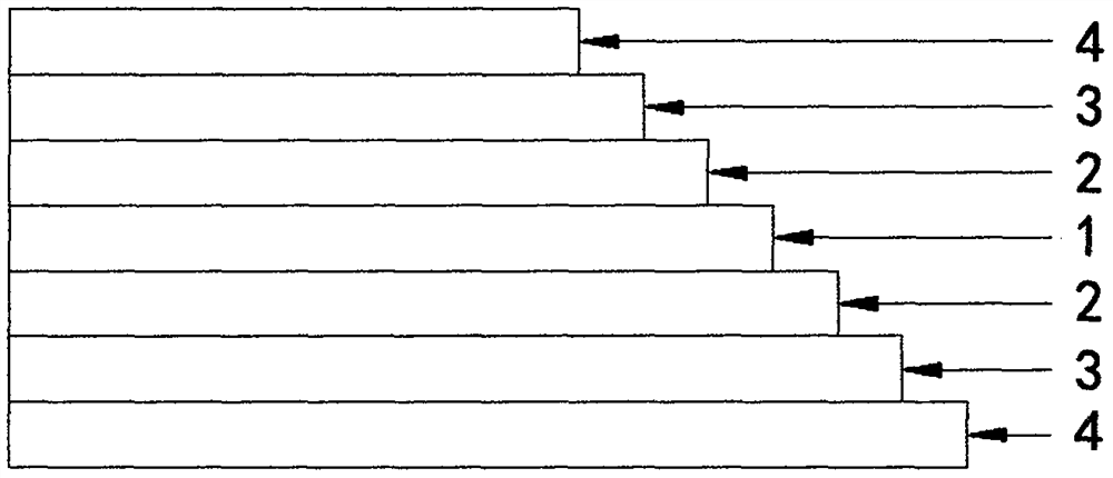
[0026] Embodiment 1: as figure 1 As shown, a conductive nano-foam comprises a polyurethane foam layer 1, the surface of the polyurethane foam layer 1 is provided with an inner nickel-plated layer 2, and the surface of the inner nickel-plated layer 2 is provided with a copper-plated layer 3, and the copper-plated layer 3 The surface is provided with an outer nickel plating layer 4. The thickness of the conductive foam is 0.1-2.0mm.
[0027] Its processing technology includes the following steps:
[0028] (1) Foam finishing: Polyurethane foam is processed and formed by punching equipment, and the hole diameter of the hole is 0.1-3.0mm;
[0029] (2) Nano-nickel plating: Nano-water nickel-plating technology, the surface of the foam is subjected to nano-nickel plating in all directions, so that the surface of the foam has high conductivity in all directions vertically;
[0030] (3) Nano-copper plating: nano-water copper plating technology, on the basis of nickel plating on the foam
Embodiment 2
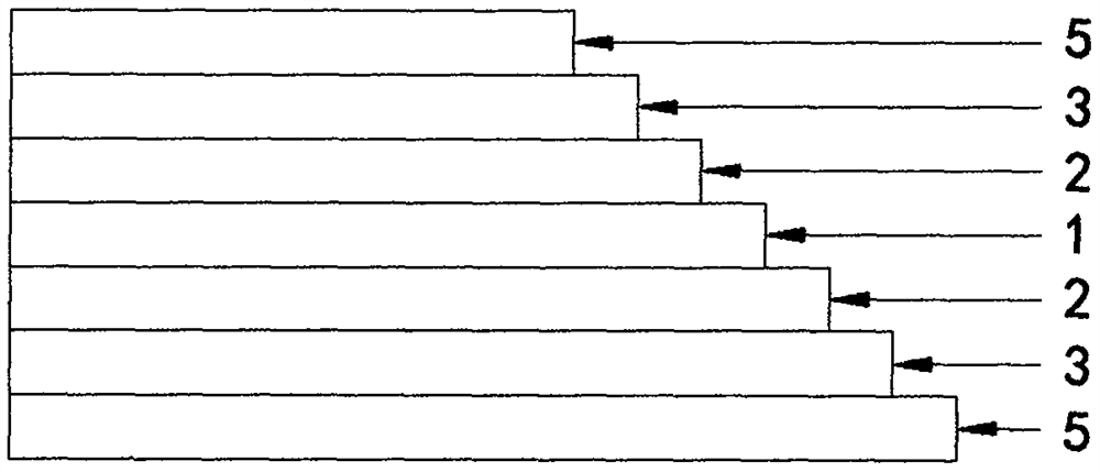
[0033] Embodiment 2: as figure 2 As shown, a conductive nano-foam comprises a polyurethane foam layer 1, the surface of the polyurethane foam layer 1 is provided with an inner nickel-plated layer 2, and the surface of the inner nickel-plated layer 2 is provided with a copper-plated layer 3, and the copper-plated layer 3. A gold-plated layer 5 is provided on the surface. The thickness of the conductive foam is 0.1-2.0mm.
[0034] Its processing technology includes the following steps:
[0035] (1) Foam finishing: Polyurethane foam is processed and formed by punching equipment, and the hole diameter of the hole is 0.1-3.0mm;
[0036] (2) Nano-nickel plating: Nano-water nickel-plating technology, the surface of the foam is subjected to nano-nickel plating in all directions, so that the surface of the foam has high conductivity in all directions vertically;
[0037] (3) Nano-copper plating: nano-water copper plating technology, on the basis of nickel plating on the foam surface,
Embodiment 3
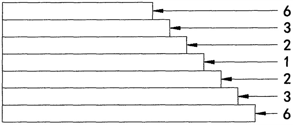
[0040] Embodiment 3: as image 3 As shown, a conductive nano-foam comprises a polyurethane foam layer 1, the surface of the polyurethane foam layer 1 is provided with an inner nickel-plated layer 2, and the surface of the inner nickel-plated layer 2 is provided with a copper-plated layer 3, and the copper-plated layer 3. A silver-plated layer 6 is provided on the surface. The thickness of the conductive foam is 0.1-2.0mm.
[0041] Its processing technology includes the following steps:
[0042] (1) Foam finishing: Polyurethane foam is processed and formed by punching equipment, and the hole diameter of the hole is 0.1-3.0mm;
[0043] (2) Nano-nickel plating: Nano-water nickel-plating technology, the surface of the foam is subjected to nano-nickel plating in all directions, so that the surface of the foam has high conductivity in all directions vertically;
[0044] (3) Nano-copper plating: nano-water copper plating technology, on the basis of nickel plating on the foam surface,
PUM
| Property | Measurement | Unit |
|---|---|---|
| Thickness | aaaaa | aaaaa |
Abstract
Description
Claims
Application Information
 - R&D Engineer
- R&D Manager
- IP Professional
- Industry Leading Data Capabilities
- Powerful AI technology
- Patent DNA Extraction
Browse by: Latest US Patents, China's latest patents, Technical Efficacy Thesaurus, Application Domain, Technology Topic.
© 2024 PatSnap. All rights reserved.Legal|Privacy policy|Modern Slavery Act Transparency Statement|Sitemap