Perovskite solar cell and preparation method thereof
A solar cell and perovskite technology, applied in the field of solar cells, can solve the problems of difficulty in significantly improving the life of perovskite solar cells, poor stability of perovskite solar cells, etc., so as to reduce interface defects, prolong life, and reduce series connection. The effect of resistance
- Summary
- Abstract
- Description
- Claims
- Application Information
AI Technical Summary
Problems solved by technology
Method used
Image

Examples
preparation example Construction
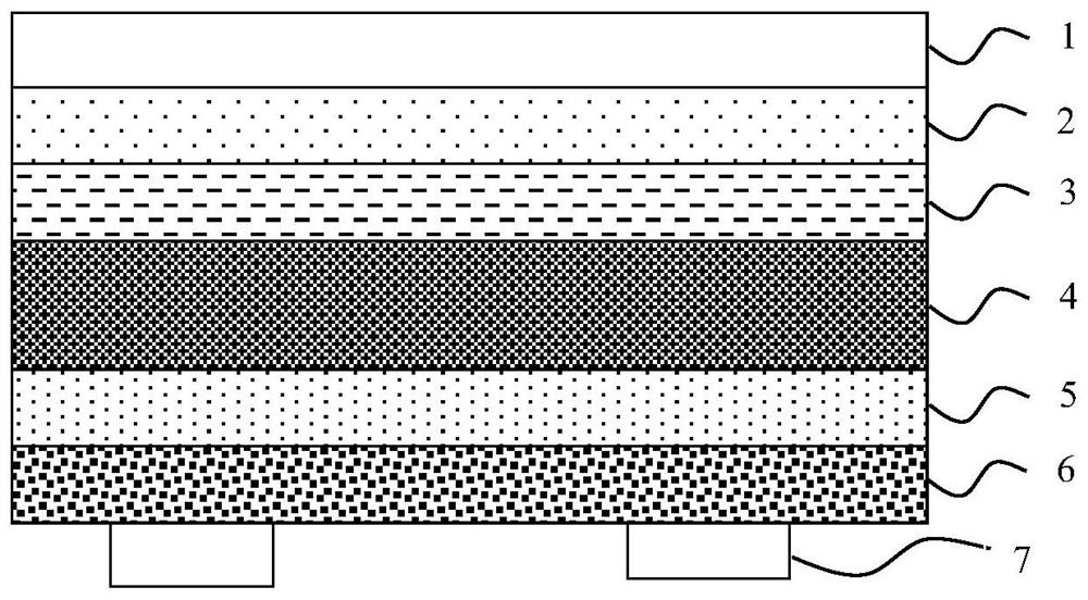
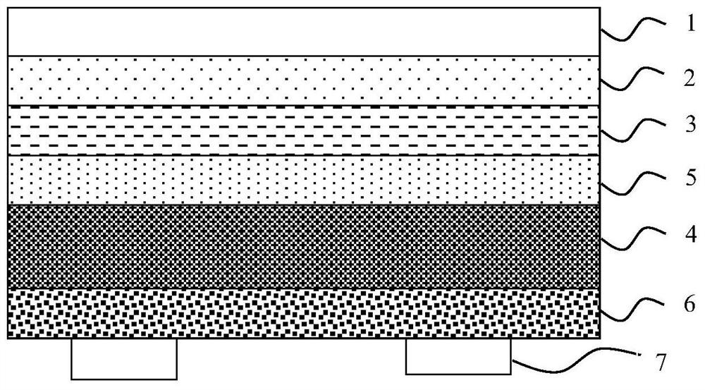
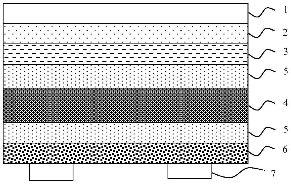
[0053] In some embodiments, a method for preparing a perovskite solar cell is provided, such as Figure 4 shown, including:
[0054] S1 provides a transparent substrate layer;
[0055] S2 provides a transparent conductive film on the transparent substrate;
[0056] S3 provides an electron transport layer on the transparent conductive film;
[0057] S4 provides a perovskite absorbing layer onto the electron transport layer;
[0058] S5 provides an interface modification layer on the perovskite absorbing layer;
[0059] S6 provides a hole transport layer on the interface modification layer;
[0060] S7 provides an electrode onto the hole transport layer.
[0061] Specifically, the transparent conductive layer is an FTO transparent conductive film, or an ITO transparent conductive film.
[0062] Specifically, the specific process for providing the electron transport layer on the transparent conductive film includes a spin-coating coating process, a magnetron sputtering coating
Embodiment 1
[0095] S1 provides a glass substrate;
[0096] S2 Deposit FTO (fluorine-doped tin oxide) transparent conductive film on the glass substrate by magnetron sputtering coating method; the thickness of the transparent conductive film is 400nm; the square resistance is 10Ω / sq; then cut into 2cm*2cm size and cleaned.
[0097] S3 Spin-coat SnO on the substrate with deposited FTO 2 Nano-ions serve as the electron transport layer. The thickness of the electron transport layer is 50nm.
[0098] S4 Spin-coat the perovskite absorber layer on the substrate of the electron transport layer in two steps. Spin-coat lead iodide solution (1.3M, DMSO:DMF=9:1), put it on a hot stage and heat it at 70°C for 1 minute after spin-coating, take out the mixed solution of FAI / MABr after cooling (FAI:MABr:MACl= 10:1:1, isopropanol solution, 60mg / mL). Immediately after the spin-coating, heat on a hot stage at 150° C. for 15 minutes. The thickness of the perovskite layer is about 560nm.
[0099] S5
Embodiment 2
[0103] The glass substrate in S1 in embodiment 1 is changed into PET organic polymer substrate, S2, S3, S4, S6, S7 are all the same as S2, S3, S4, S6, S7 in embodiment 1 in this embodiment are the same;
[0104] S5 Spin coating on the perovskite absorbing layer to prepare the dibenzo-18-crown-6 interface modification layer. Use a pipette gun to draw 70 μL of dibenzo-18-crown-6 solution (isopropanol solution, 20 mg / mL), spin-coat at 3000 rpm for 30 s, and then perform annealing at 180° C. for 10 minutes.
PUM
 Abstract
Description
Claims
Application Information
 - R&D Engineer
- R&D Manager
- IP Professional
- Industry Leading Data Capabilities
- Powerful AI technology
- Patent DNA Extraction
Browse by: Latest US Patents, China's latest patents, Technical Efficacy Thesaurus, Application Domain, Technology Topic.
© 2024 PatSnap. All rights reserved.Legal|Privacy policy|Modern Slavery Act Transparency Statement|Sitemap