Method for improving reliability of gate oxide layer in SiC field effect transistor

A technology of field effect transistors and gate oxide layers, which is applied in semiconductor devices, semiconductor/solid-state device manufacturing, electrical components, etc., can solve the problems of low reliability of middle gate oxide layers and poor performance of SiC field effect transistors, and achieve compactness Effects of enhancement, interface quality optimization, and reliability improvement

Pending Publication Date: 2022-07-22
INST OF MICROELECTRONICS CHINESE ACAD OF SCI
View PDF0 Cites 0 Cited by
  • Summary
  • Abstract
  • Description
  • Claims
  • Application Information

AI Technical Summary

Benefits of technology

This patented technology helps improve the stability of silicon carbide (Si) MOSFET' s gate insulation layers by reducing these problems caused during manufacturing processes or use under specific conditions. By performing this treatment twice with various gas mixtures over several hours before finalizing it, we aimed towards optimising its properties such as preventing impurities from entering the device that could cause damage. Additionally, there was also some improvement on how well the gate dielectric coating works when exposed to certain chemical substances like hydrogen sulfite solution. Overall, our technical results help enhance the overall function of SiCMOS devices while maintain their original design feature.

Problems solved by technology

The technical problem addressed by this patented text relates to improving the quality of silicone layers used during manufacturing processes on SiC materials that have potential limitations with regards to their electrical characteristics or ability to handle higher voltages without losing functionality over time.

Method used


Image

  • Method for improving reliability of gate oxide layer in SiC field effect transistor
  • Method for improving reliability of gate oxide layer in SiC field effect transistor
  • Method for improving reliability of gate oxide layer in SiC field effect transistor

Examples


Embodiment Construction

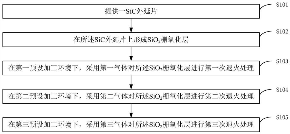
[0038] The technical solutions in the embodiments of the present invention will be clearly and completely described below with reference to the accompanying drawings in the embodiments of the present invention. Obviously, the described embodiments are only a part of the embodiments of the present invention, but not all of the embodiments. Based on the embodiments of the present invention, all other embodiments obtained by those of ordinary skill in the art without creative efforts shall fall within the protection scope of the present invention.

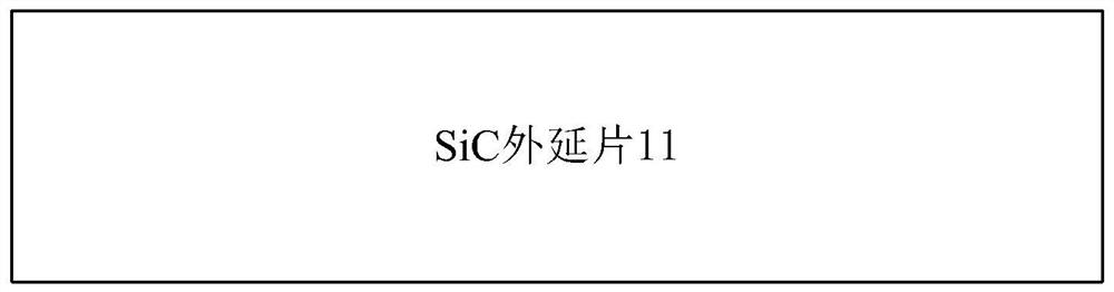
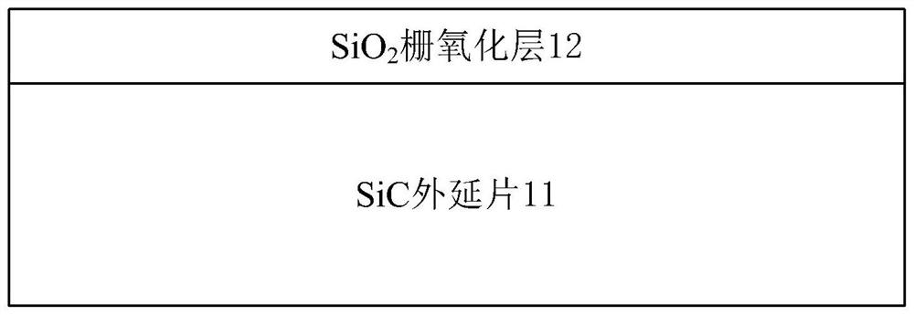
[0039] During the invention and creation process of the present invention, the inventor found that in the SiC field effect transistor, due to the SiO2 in the growth process 2 And the problem of lattice mismatch of SiC material, in SiO 2 SiO for gate oxide 2 A large number of trapped charges such as dangling bonds, carbon clusters and oxygen vacancies will be generated in the interface and the SiC interface of the SiC epitaxial layer, wh


PUM


Abstract

The invention provides a method for improving the reliability of a gate oxide layer in a SiC field effect transistor, and the method comprises the steps: carrying out the three times of annealing treatment on a SiO2 gate oxide layer through employing different gases in three processing environments, so as to reduce the C-related defects at the interface of the SiO2 gate oxide layer. That is to say, through three times of continuous annealing treatment, various traps and defects at the interface of the SiO2 gate oxide layer in the SiC field effect transistor can be removed, the interface quality is optimized, the compactness is enhanced, the leakage current is reduced, the reliability is improved, and the performance of the SiC field effect transistor is further improved.

Description


Claims


Application Information

Patent Timeline
Owner INST OF MICROELECTRONICS CHINESE ACAD OF SCI
Why Eureka
Try Eureka