Method for preparing P type ZnO ohmic electrode
A technology of electrodes and electrode materials, which is applied in the manufacture of circuits, electrical components, semiconductors/solid-state devices, etc., can solve problems that affect the performance and stability of devices, it is difficult to explain the ohmic characteristics of electrodes, and poor adhesion of materials, etc., to achieve reduction Poor adhesion, avoiding changes in structure and physical and chemical properties, and protecting electrodes
- Summary
- Abstract
- Description
- Claims
- Application Information
AI Technical Summary
Benefits of technology
Problems solved by technology
Method used
Image

Examples
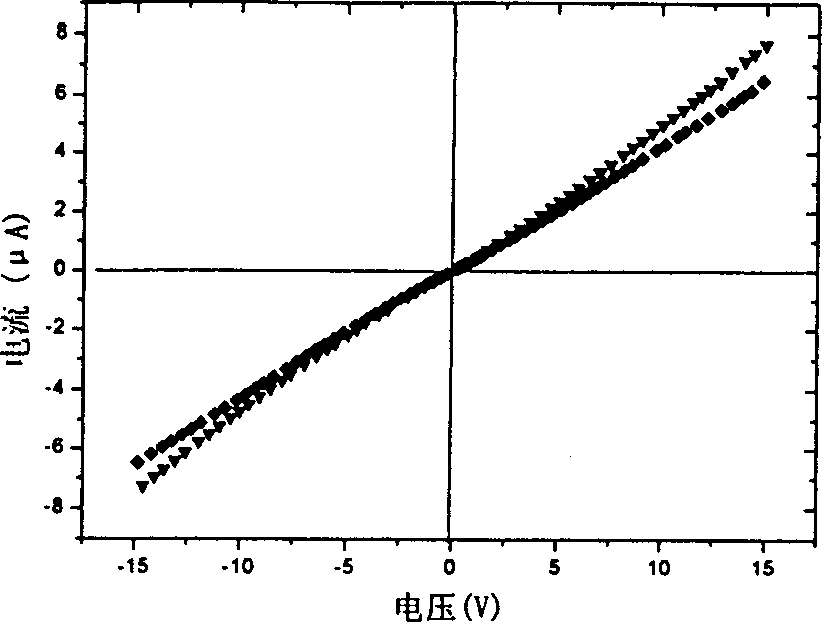
Embodiment 1
[0014] Example 1, on high-resistance p-type ZnO, after evaporating Ni and Au, rapid thermal annealing is carried out at 200° C. or 300° C. in nitrogen for 150 seconds.
[0015] Selection of experimental conditions:
[0016] The p-type ZnO flakes were grown on sapphire (Al) by molecular beam epitaxy (MBE). 2 o 3 ) on nitrogen-doped high-resistance p-type ZnO with an area of about 1 cm 2 , and its resistivity is about 60Ω·cm.
[0017] Firstly, the p-type ZnO sheet was cleaned by ultrasonic cleaning with acetone and absolute ethanol for 5 minutes; rinsed with deionized water and washed with dry N 2 blow dry. The thickness is 0.2mm and the area is 6×6cm 2 The tantalum sheet is used as a metal mask, and two areas of 1mm are formed on the tantalum sheet by machining. 2 A circular hole is used as the shape of the electrode, the distance between the two electrodes is 2mm, the distance between the mask plate and the evaporation source is 12cm, and the purity of Ni and Au is 99.99%
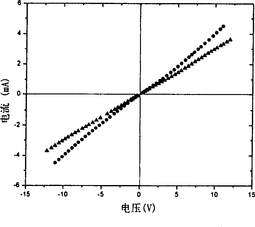
Embodiment 2
[0019] Example 2, on the low-resistance p-type ZnO, after evaporating Ni and Au, rapid thermal annealing is carried out at 300° C. or 400° C. in nitrogen for 150 seconds.
[0020] The p-type ZnO flakes were grown on sapphire (Al) by molecular beam epitaxy (MBE). 2 o 3 ) on nitrogen-doped low-resistance p-type ZnO, with an area of about 1cm 2 , and its resistivity is about 4Ω·cm.
[0021] Firstly, the p-type ZnO sheet was cleaned by ultrasonic cleaning with acetone and absolute ethanol for 5 minutes; rinsed with deionized water and washed with dry N 2 blow dry. The thickness is 0.2mm and the area is 6×6cm 2 The tantalum sheet is used as a metal mask, and two areas of 1mm are formed on the tantalum sheet by machining. 2 The shape of the circular hole is used as the electrode, the distance between the two electrodes is 2mm, and the distance between the mask plate and the evaporation source is 12cm. Ni and Au are 99.99% pure. The vacuum degree during vacuum evaporation is 5.
PUM
| Property | Measurement | Unit |
|---|---|---|
| Area | aaaaa | aaaaa |
| Resistivity | aaaaa | aaaaa |
| Resistivity | aaaaa | aaaaa |
Abstract
Description
Claims
Application Information
 - R&D Engineer
- R&D Manager
- IP Professional
- Industry Leading Data Capabilities
- Powerful AI technology
- Patent DNA Extraction
Browse by: Latest US Patents, China's latest patents, Technical Efficacy Thesaurus, Application Domain, Technology Topic.
© 2024 PatSnap. All rights reserved.Legal|Privacy policy|Modern Slavery Act Transparency Statement|Sitemap