Film substrate, semiconductor device, method of manufacturing film substrate, method of manufacturing semiconductor device and method of manufacturing circuit board with semiconductor device

a technology of semiconductor devices and film substrates, which is applied in the direction of printed circuit components, printed circuit manufacturing, printed circuit assembling, etc., can solve the problems of difficult handling of film substrate pieces, difficult to achieve the improvement of productivity through automation, and not meeting the needs of miniaturization

Inactive Publication Date: 2005-02-10
KK TOSHIBA
View PDF1 Cites 1 Cited by
  • Summary
  • Abstract
  • Description
  • Claims
  • Application Information

AI Technical Summary

Benefits of technology

The technical effect described in this patented technology relates to improving production efficiency by optimizing certain processes for producing products with specific qualities or characteristics.

Problems solved by technology

This technical problem addressed in the present patents relates to improving the efficiency and productiveness of manufacturing electronic devices through integration into larger circuits without separating them manually during processing. Current methods require manual manipulation of each component separately due to their complexity and difficulty in achieving precise placement.

Method used


Image

  • Film substrate, semiconductor device, method of manufacturing film substrate, method of manufacturing semiconductor device and method of manufacturing circuit board with semiconductor device
  • Film substrate, semiconductor device, method of manufacturing film substrate, method of manufacturing semiconductor device and method of manufacturing circuit board with semiconductor device
  • Film substrate, semiconductor device, method of manufacturing film substrate, method of manufacturing semiconductor device and method of manufacturing circuit board with semiconductor device

Examples


Embodiment Construction

[0049] The embodiment of the present invention will be described below with reference to the accompanying drawings.

[0050] First, the manufacturing method according to the embodiment will be described with reference to FIG. 1A and FIG. 1B to FIG. 13A and FIG. 13B.

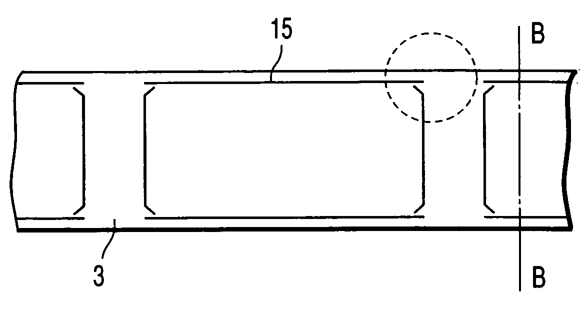
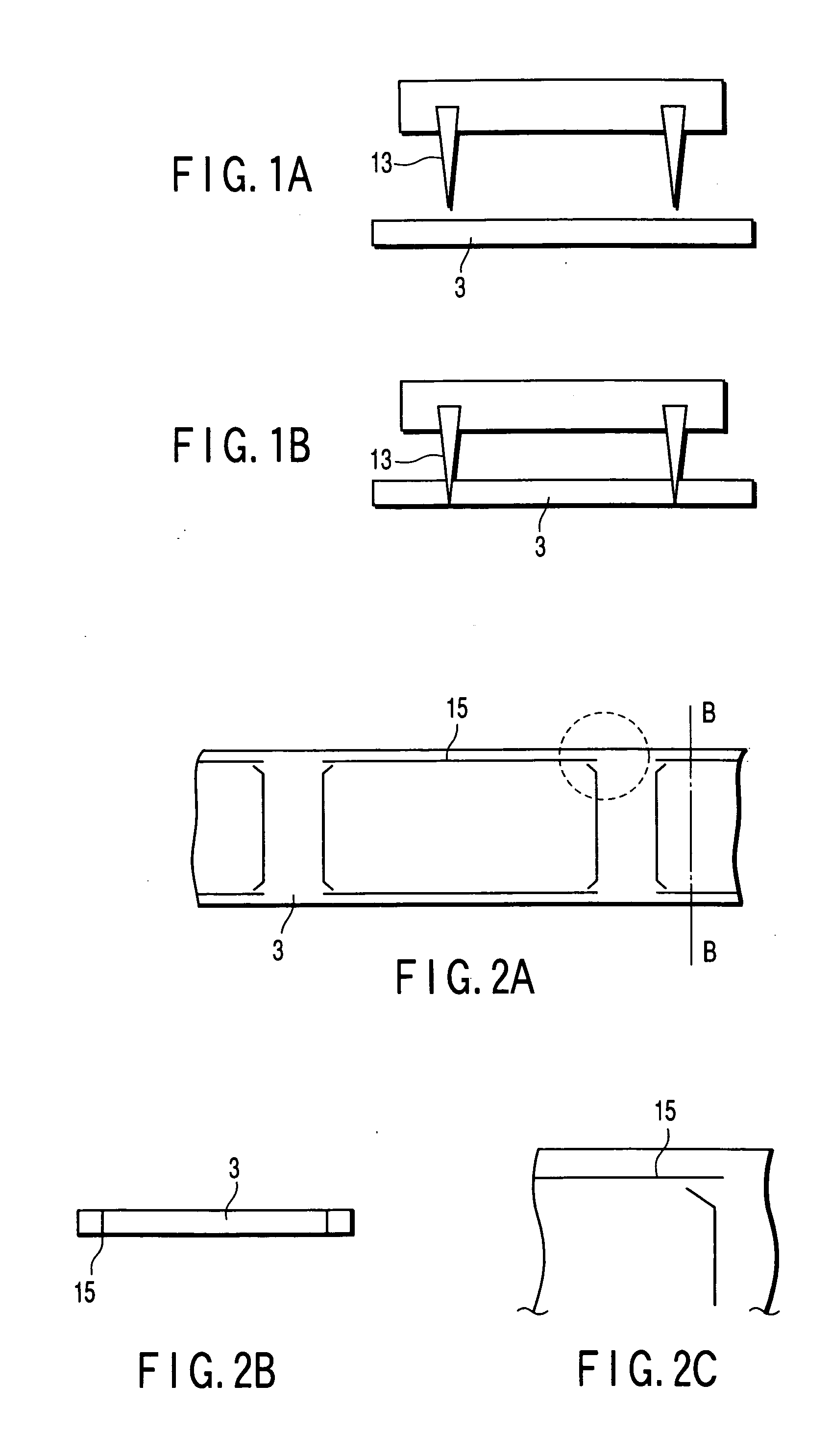
[0051] As illustrated in FIG. 1A and FIG. 1B, a slit is formed in a tape-like insulative film (which corresponds to insulative sheet) 3 such as polyimide and PET (polyester terephthalate) using a metal blade (e.g., Thomson blade) 13 so as to penetrate through the insulative film 3.

[0052]FIG. 2A is a plan view showing the insulative film 3 with a slit 15, FIG. 2B is a cross-sectional view taken along a line B-B of FIG. 2A, and FIG. 2C is an enlarged view showing a circle shown by the broken line of FIG. 2A. As seen from FIG. 2A, the slit 15 is formed partially along the outer peripheral line (outline) of a separating region (finally necessary region), which will be separated. That is, the slit 15 is not formed over the entire


PUM


Abstract

Disclosed is a film substrate comprising an insulative sheet including a first region to be separated, having a slit on an outer peripheral line of the first region, and on which a semiconductor device chip is to be mounted, and a conductive pattern formed on the insulative sheet, crossing the slit, and to be connected to an external terminal of the semiconductor device chip.

Description


Claims


Application Information

Patent Timeline
Owner KK TOSHIBA
Why Eureka
Try Eureka