Circuit and method for test mode entry of a semiconductor memory device

a technology of semiconductor memory and test mode, applied in the direction of information storage, static storage, digital storage, etc., can solve the problem of 2/b> being difficult to secur

Inactive Publication Date: 2006-05-04
SAMSUNG ELECTRONICS CO LTD
View PDF3 Cites 5 Cited by
  • Summary
  • Abstract
  • Description
  • Claims
  • Application Information

AI Technical Summary

Benefits of technology

This patented technology allows for testing certain components within electronic devices by generating signals that match their timing with those from another source outside or inside them. These tests can be done during normal operation but they are limited because it requires specific conditions like time between two events.

Problems solved by technology

Technical Problem: The technical problem addressed in this patents relates to improving testing performance during electronic devices' operations where they operate within specifications due to factors like temperature variations affects their ability to accurately access various types of tests modes through a corresponding interface called a test key sequence generator (TFT). Additionally, there needs to ensure proper functioning of these interfaces even if the temperatures change frequently over multiple cycles without compromising any other functionality being tested.

Method used


Image

  • Circuit and method for test mode entry of a semiconductor memory device
  • Circuit and method for test mode entry of a semiconductor memory device
  • Circuit and method for test mode entry of a semiconductor memory device

Examples


Embodiment Construction

[0056] It will be understood that, although the terms “first”, “second”, etc. may be used herein to describe various elements, these elements should not be limited by these terms. These terms are used to distinguish one element from another. For example, a first element could be termed a second element, and, similarly, a second element could be termed a first element, without departing from the scope of the present invention. As used herein, the term “and / or” includes any and all combinations of one or more of the associated listed items.

[0057] It will be understood that when an element is referred to as being “connected” or “coupled” to another element, it can be directly connected or coupled to the other element or intervening elements may be present. In contrast, when an element is referred to as being “directly connected” or “directly coupled” to another element, there are no intervening elements present. Other words used to describe the relationship between elements should be i


PUM


Abstract

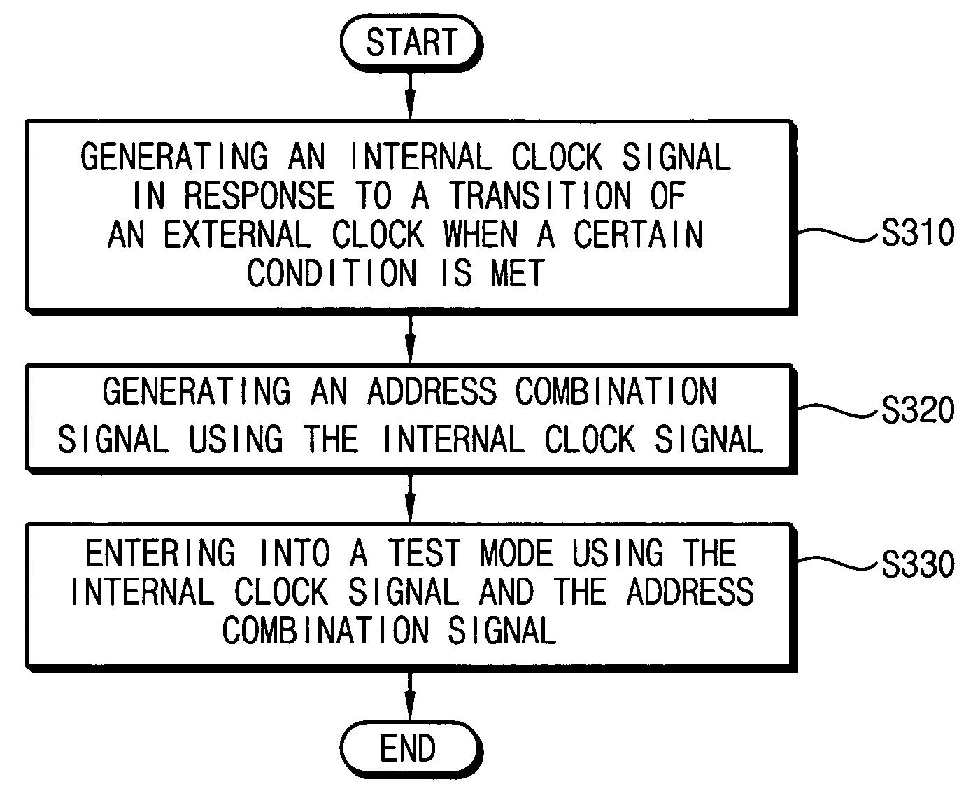
A circuit and method for test mode entry of a semiconductor memory device are provided. In a method of entering a semiconductor memory device into a test mode, an internal clock is generated in response to an external clock when a first condition is satisfied. An address combination signal is generated based on a first address combination and the internal clock. The semiconductor memory device is entered into the test mode using the internal clock and the address combination signal.

Description


Claims


Application Information

Patent Timeline
Owner SAMSUNG ELECTRONICS CO LTD
Why Eureka
Try Eureka