Touch panel

Inactive Publication Date: 2007-08-09
PANASONIC CORP
View PDF7 Cites 134 Cited by
  • Summary
  • Abstract
  • Description
  • Claims
  • Application Information

AI Technical Summary

Benefits of technology

[0017]Provided is a touch panel, which does not require adjustment of a size and amount of electrically conductive particles contained in an anisotropic conductive adhesive, or thorough stirring of the same before it is applied to form anisotropic conductive adhesive layer, and therefore it is easy to produce and based on a voltage ratio of upper electrodes 105 and another voltage ratio of lower electrodes 106, and it switches various functions of the electronic apparatus accordingly.
[0019]The secured area at the terminal portion of wiring substrate 108 is then heated and pressed over the front surface of upper substrate 101 and the back surface of lower substrate 102 by using a jig or the like tooling. This process softens adhesive layer 111 coated on the terminal portion of any of the back surface of upper substrate 101, front surface of lower substrate 102 and wiring substrate 108. Adhesive layer 111 hardens thereafter to bond and connect the upper electrodes 105 and the terminal portion of patterns 109. The hardened adhesive layer 111 also bond and connect lower electrodes 106 and the terminal portion of patterns 110. Touch panel 100 connected with wiring substrate 108 is hence manufactured.
[0021]The touch panel of the present invention includes a first substrate of optical transparency, a second substrate of optical transparency, a wiring substrate, and an anisotropic conductive adhesive layer. The first substrate has a first surface, a first conductive layer formed at the first surface, and first electrodes formed in a manner to extend from two opposite sides of the first conductive layer. The second substrate has a second surface, a second conductive layer formed at the second surface in a manner to confront the first surface with a space, and second electrodes formed in a manner to extend from two opposite sides of the second conductive layer in a direction orthogonal to two opposite sides of the first conductive layer at which first electrodes formed. The wiring substrate has a third surface, a fourth surface, and a plurality of wiring patterns formed on at least one of the third surface and the fourth surface. The anisotropic conductive adhesive layer connects a terminal portion of the wiring patterns to at least one of the first electrodes and the second electrodes. The wiring substrate is provided with any of a slit and an aperture between the wiring patterns formed at one end thereof. This structure provides the touch panel which is easy to produce while it also ensures reliable operation and electrical connection and separation.

Problems solved by technology

Such a phenomenon of short-circuiting, if occurs, may impair the electrical insulation between the electrodes or the wiring patterns, thereby resulting in instability of electrical connection and separation or operation of touch panel 100.
Any of the above makes the process of manufacturing touch panels 100 complicated.

Method used


Image

  • Touch panel
  • Touch panel
  • Touch panel

Examples


Embodiment Construction

[0034]Description is provided hereinafter of an exemplary embodiment of the present invention with reference to FIG. 1 to FIG. 7.

Exemplary Embodiment

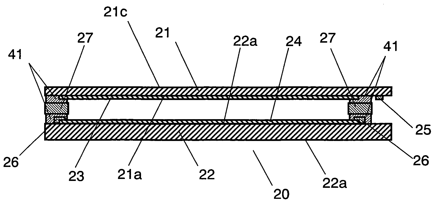
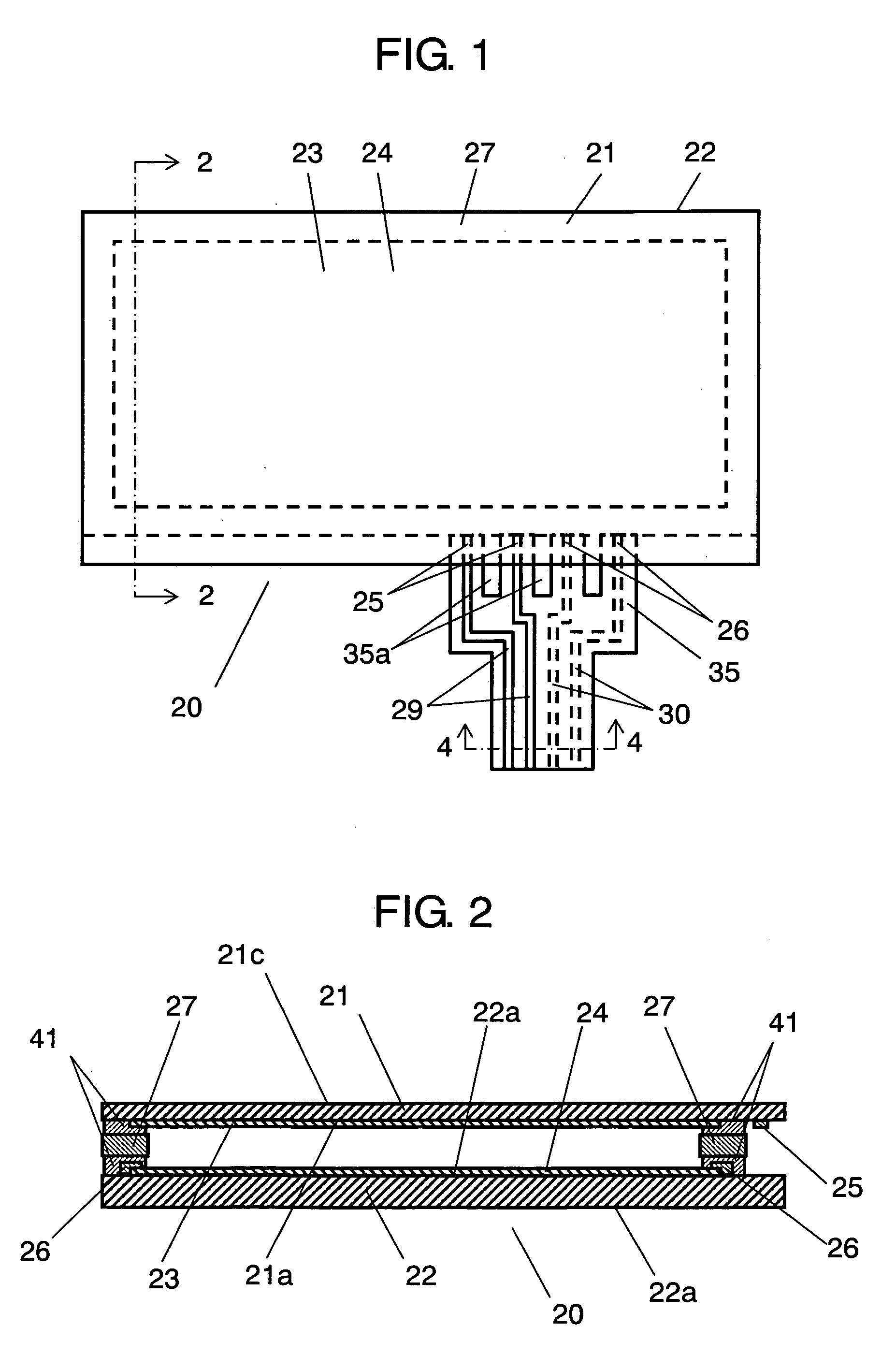
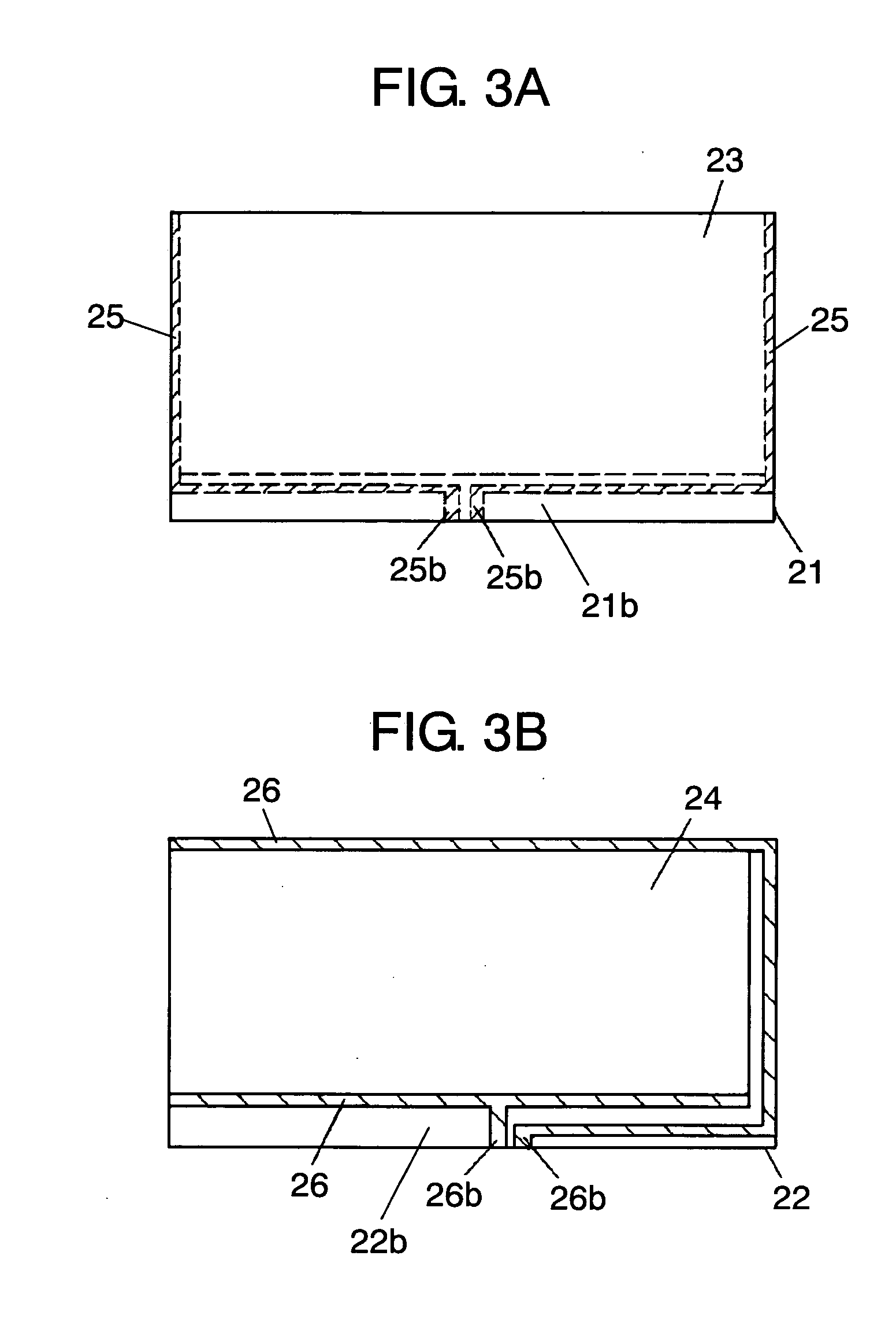
[0035]FIG. 1 is a plan view of a touch panel according to an exemplary embodiment of the present invention. FIG. 2 is a sectional view of a cross section taken along the line 2-2 of the touch panel shown in FIG. 1. FIG. 3A is a plan view of a first substrate used for the touch panel shown in FIG. 1. FIG. 3B is a plan view of a second substrate used for the touch panel shown in FIG. 1. FIG. 4 is a sectional view of a cross section taken along the line 4-4 of the touch panel shown in FIG. 1. FIG. 5 is a cutaway view of a main portion of the touch panel shown in FIG. 1. FIG. 6A is a plan view of a wiring substrate used for the touch panel shown in FIG. 1.

[0036]In FIG. 1 to FIG. 6A, an upper substrate defining first substrate 21 (hereafter referred to as substrate 21) has a film-like form and optical transparency, and it is formed of an opt...


PUM


Abstract

A touch panel includes a first substrate, a second substrate, a wiring substrate provided with a plurality of wiring patterns formed thereon, and an anisotropic conductive adhesive layer. The first substrate has a first conductive layer and first electrodes extending from two opposite sides of the first conductive layer. The second substrate has a second conductive layer confronting the first surface with a space, and second electrodes extending from two opposite sides of the second conductive layer. The anisotropic conductive adhesive layer connects a terminal portion of the wiring patterns to at least one of the first electrodes and the second electrodes. The wiring substrate has a slit or an aperture between the wiring patterns at one end thereof. The touch panel of this structure is easy to produce, and provides reliable operation and electrical connection and separation.

Description

BACKGROUND OF THE INVENTION[0001]1. Field of the Invention[0002]The present invention relates to a touch panel used to operate a variety of electronic apparatuses.[0003]2. Background Art[0004]Following the advancement in recent years of various electronic apparatuses such as mobile phones, car navigation systems and the like toward high performance and diversification, there is a continuous growth in number of the electronic apparatuses equipped with optically transparent touch panels in front of their display devices such as liquid crystal panels. A user of any such electronic apparatus operates it by pressing a touch panel with a finger, a pen, or the like tool while visually observing through the touch panel a screen on the display device provided behind the touch panel. Operation of the electronic apparatus is switched in this manner from one function to another. A demand thus exists for such touch panels that are superior in visibility and reliable in operation.[0005]With refer...

Claims


Application Information

Patent Timeline
IPC IPC(8): G06F3/041
CPCG06F3/0416G06F3/045G06F3/04164
Inventor FUJII, SHOJITANABE, KOJI
Owner PANASONIC CORP
Why Eureka
Try Eureka