High-voltage-withstanding semiconductor device and fabrication method thereof

a high-voltage-resistance semiconductor and fabrication method technology, applied in semiconductor devices, semiconductor device details, electrical apparatus, etc., can solve the problems of not paying attention to the need to avoid plasma damage in a high-voltage-resistance semiconductor device, the semiconductor device's insulation film is susceptible to plasma damage, and the need to resist plasma damage, etc., to suppress the dispersion of vt fluctuation, avoid operation failure, and suppress the effect of vt fluctuation

Inactive Publication Date: 2008-05-15
LAPIS SEMICON CO LTD
View PDF1 Cites 0 Cited by
  • Summary
  • Abstract
  • Description
  • Claims
  • Application Information

AI Technical Summary

Benefits of technology

The present invention provides a type of power supply circuit called High Voltage Power Supplies (HVPS) which has improved performance over previous designs without adding extra components or increasing manufacturing costs. By designing differences between certain areas on each transistor's surface where they are located, these variations affect how well other parts work together when used at different voltages. This helps prevent excessive voltage stress during operation while maintaining good electrical characteristics across all devices connected through wires.

Problems solved by technology

This technical problem addressed in this patents relates to prevention of ionic damages caused by plasmas when manufacturing highly integrated devices without increasing their size beyond certain limits.

Method used


Image

  • High-voltage-withstanding semiconductor device and fabrication method thereof
  • High-voltage-withstanding semiconductor device and fabrication method thereof
  • High-voltage-withstanding semiconductor device and fabrication method thereof

Examples


Embodiment Construction

[0029]One exemplary embodiment of a high-voltage-withstanding semiconductor device of the invention and its fabrication method will be explained below with reference to the drawings.

[NOMS Transistor]

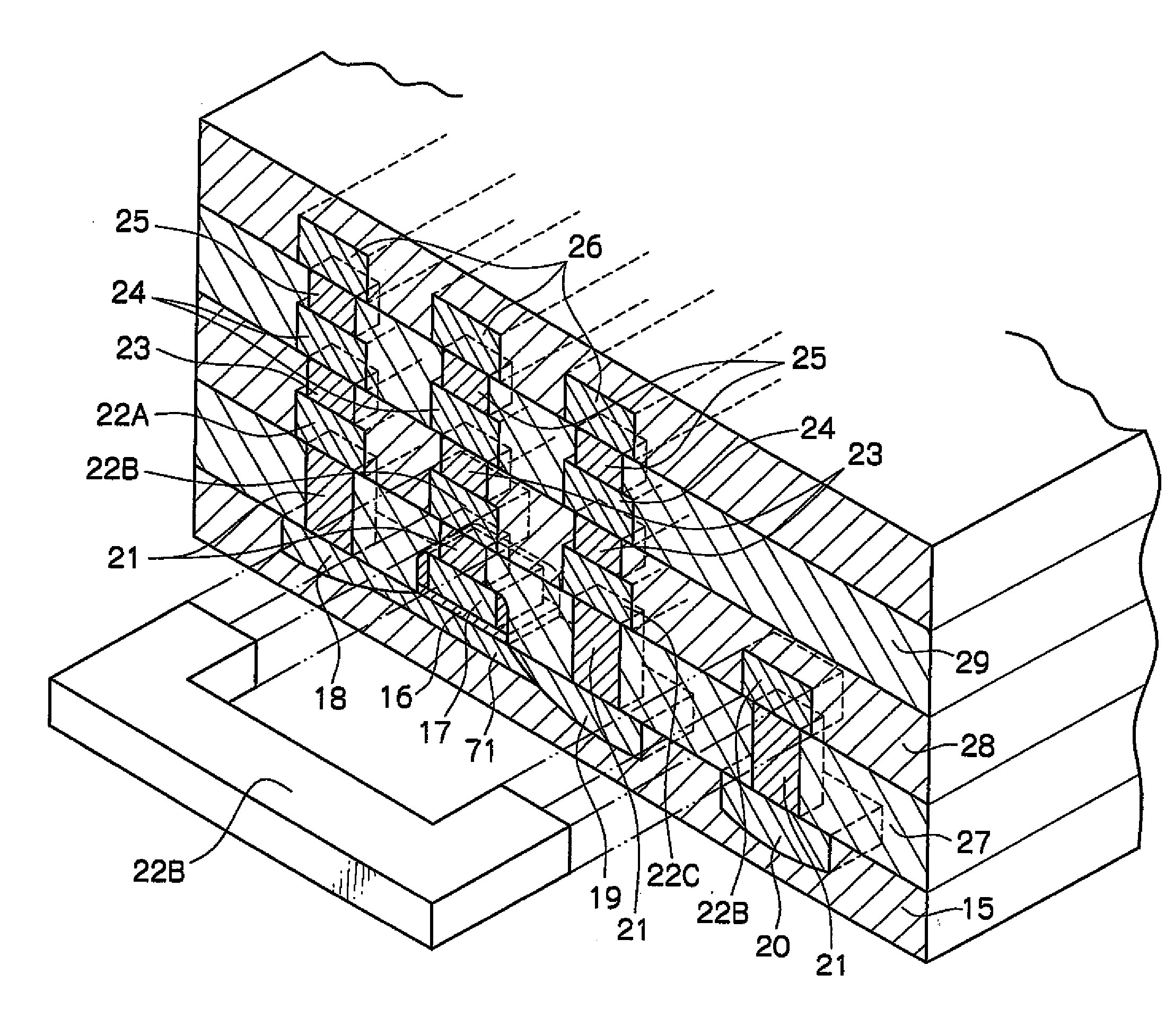
[0030]FIG. 1 is a schematic diagram of a high-voltage-withstanding semiconductor device using a NMOS transistor of the invention.

[0031]The high-voltage-withstanding semiconductor device is fabricated through the following processing steps.

[0032]A semiconductor substrate having a first conductive transistor forming region and a first conductive diode forming region in a surface layer region thereof is prepared.

[0033]Here, the first conductive transistor forming region is formed at a region different from the first conductive diode-forming region. A distance between the transistor forming region and the diode forming region is not specifically defined as long as they are apart from each other by a degree of exhibiting functions of transistor and diode, respectively.

[0034]The transistor is for


PUM


Abstract

There is provided a high-voltage-withstanding semiconductor device a fabrication method thereof capable of suppressing Vt fluctuation induced by plasma damage in a via hole forming step. In the high-voltage-withstanding semiconductor device, a gate electrode of a transistor having a gate insulating film formed on a semiconductor substrate and having a thickness of 350 Å or more and a diode composed of a first conductive well region formed in a surface layer region of the semiconductor substrate and a second conductive diffusion layer formed in the surface layer region of the semiconductor substrate and on the well region are electrically connected by a wire directly connected to contacts formed respectively on the gate electrode and the diode, via the contacts.

Description


Claims


Application Information

Patent Timeline
Owner LAPIS SEMICON CO LTD
Why Eureka
Try Eureka