Power converter for traction control and transportation system
a technology of power converter and transportation system, applied in the field of power converter, can solve the problems of inability to accurately complicated system, and inability to detect voltage drop due to actual diode temperature rise, etc., to achieve accurate temperature estimation, simple circuitry, and easy temperature estimation
- Summary
- Abstract
- Description
- Claims
- Application Information
AI Technical Summary
Benefits of technology
Problems solved by technology
Method used
Image

Examples
first embodiment
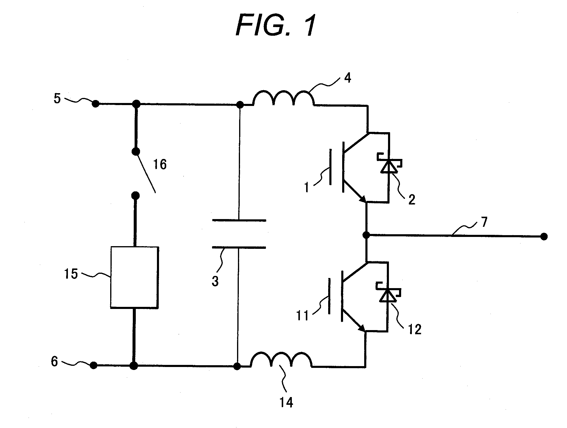
[0052]FIG. 1 illustrates the basic configuration of an inverter circuit included in a power converter to which the invention is applied. In FIG. 1, reference numeral 1 is a first switching element; 2 is a first Schottky diode; 3 is a smoothing capacitor; 4 is a positive inductance; 5 is a circuit positive terminal; 6 is a circuit negative terminal; 7 is a inverter output terminal; 11 is a second switching element; 12 is a second Schottky diode; 14 is a negative inductance; 15 is a first impedance; and 16 is a first shut-off switch.
[0053]In the inverter circuit obtained by combining the diodes 2, 12 and switching elements 1, 11 illustrated in FIG. 1, the power of the inverter output terminal 7 is controlled by complementarily switching the first switching element 1 and the second switching element 11. Power converters, such as inverters, converters, or step-up / down choppers, are formed by combining the above circuit and the smoothing capacitor 3 with the inductances 4, 14 existing in
second embodiment
[0071]FIG. 4 illustrates a second embodiment of the invention. FIG. 4 illustrates a temperature estimation circuit in which the first switching element 1 is used as a semiconductor device for temperature estimation. Reference numeral 133 is a collector terminal and 134 is a emitter terminal.
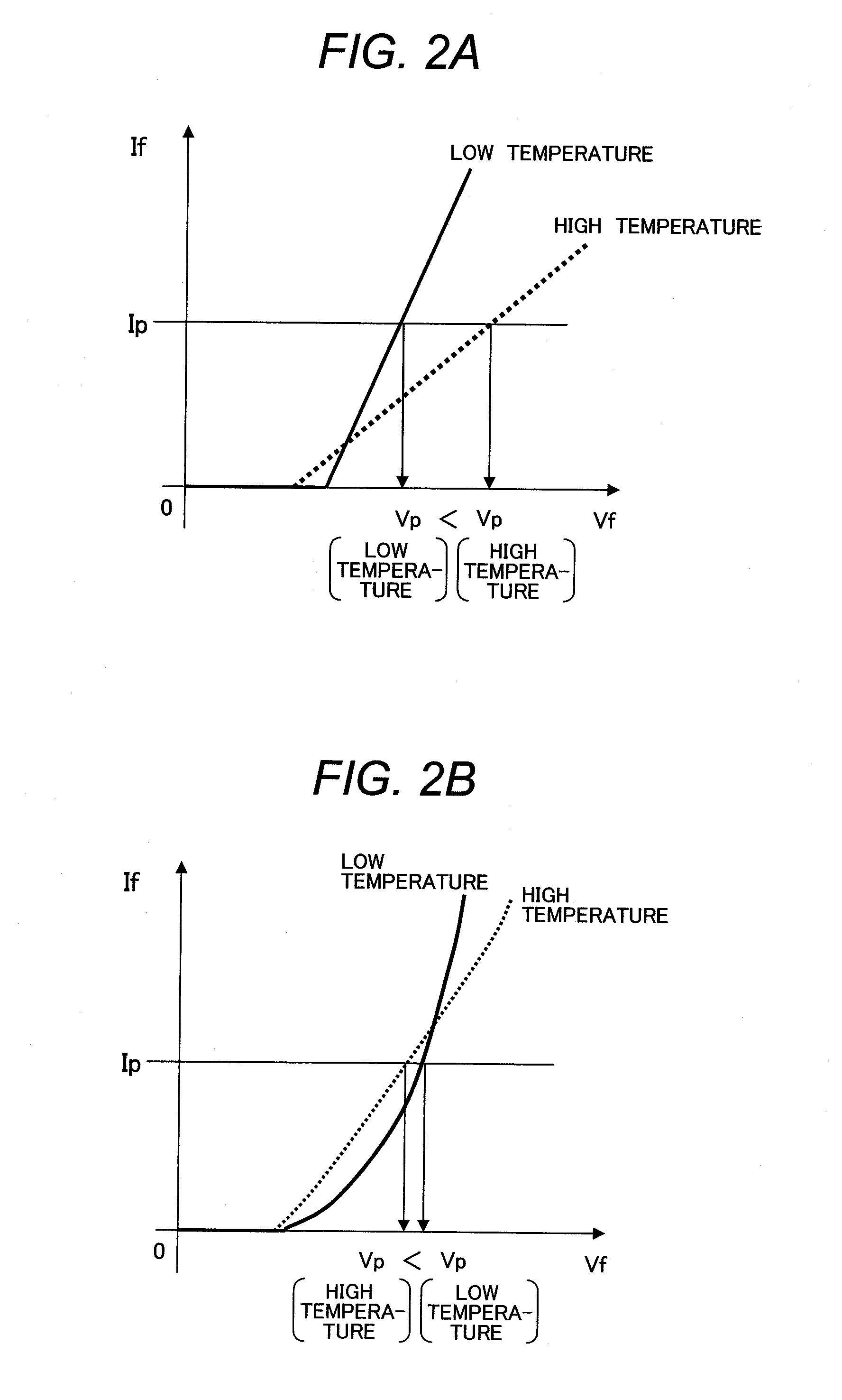
[0072]When the first switching element 1 is, for example, IGBT, in conventional cases with Si, the band gap is low and voltage is reduced in operation at large current. However, use of a wide-band gap semiconductor device using a compound semiconductor of SiC, GaN, or the like large in the temperature coefficient of voltage drop as in the invention increases voltage drop during conduction.
[0073]Since the temperature coefficient of voltage drop during conduction is large as compared with Si, variation in voltage between collector and emitter during gate on is increased relative to temperature change. The estimated temperature of the semiconductor device can be computed by providing this phenomenon in
third embodiment
[0076]FIG. 5 illustrates a third embodiment of the invention. FIG. 5 shows an example in which the temperature estimation circuit in FIG. 3 and FIG. 4 is applied to an inverter circuit. With respect to particulars that overlap with the contents described in relation to the first and second embodiments, the description thereof will be omitted and a difference will be described below.
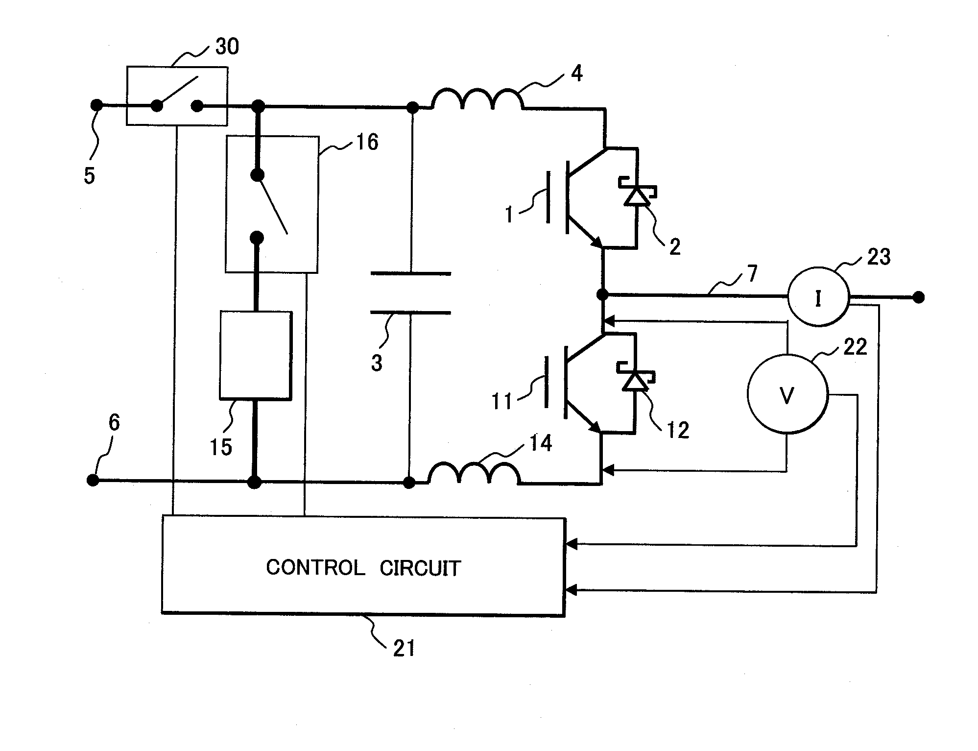
[0077]In FIG. 5, reference numeral 15 is a first impedance; 16 is a first shut-off switch; 21 is a control circuit; 22 is a voltage measurement circuit; 23 is a current measurement circuit; and 30 is a second shut-off switch.
[0078]In the third embodiment, the voltage measurement circuit 22 measures a potential difference between the inverter output terminal 7 and the negative pole side. For this reason, semiconductor device such as, a semiconductor device using a wide-band gap semiconductor adopting a compound semiconductor of SiC, GaN, or the like having large temperature coefficient of voltage drop, descri
PUM
 Abstract
Description
Claims
Application Information
 - R&D Engineer
- R&D Manager
- IP Professional
- Industry Leading Data Capabilities
- Powerful AI technology
- Patent DNA Extraction
Browse by: Latest US Patents, China's latest patents, Technical Efficacy Thesaurus, Application Domain, Technology Topic.
© 2024 PatSnap. All rights reserved.Legal|Privacy policy|Modern Slavery Act Transparency Statement|Sitemap