Liquid crystal display device
- Summary
- Abstract
- Description
- Claims
- Application Information
AI Technical Summary
Benefits of technology
Problems solved by technology
Method used
Image

Examples
example 1
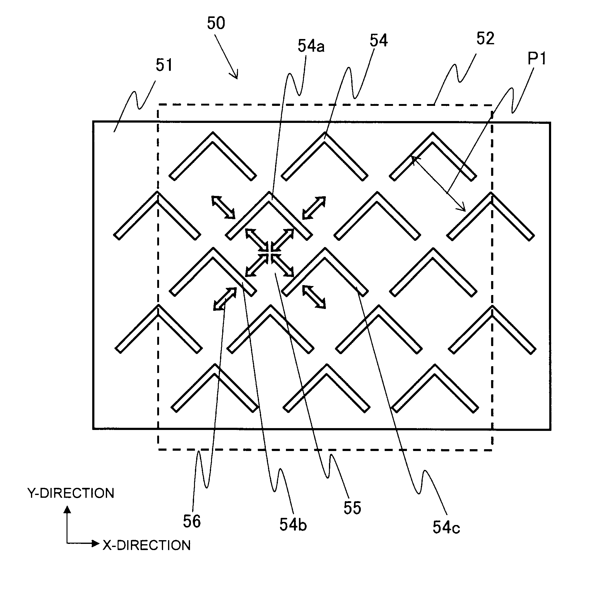
[0132]The above liquid crystal 2 was applied to the vertical alignment type liquid crystal display device capable of multiplex driving in this embodiment as described above, whereby a liquid crystal display device of Example 1 was prepared. The electrode structure of a pixel of the liquid crystal display device of Example 1 was made to be the same as the first example of the second electrode form applicable to the vertical alignment type liquid crystal display device in this embodiment, as shown in FIG. 10. In such a case, the size of one pixel was 0.39 mm square, the pitch for forming sub-pixels was 80 μm, and each linear slit width was made to be 10 μm. The panel specific resistance was 4.6×10¹⁰ Ωcm. Using the vertical alignment type liquid crystal display device of Example 1, static electricity was applied to the substrate surface for displaying the liquid crystal layer, whereby the time until electrostatic charge was resolved, was 5 seconds and thus was found to be a very short tim
example 2
[0135]The above liquid crystal 2 was applied to the vertical alignment type liquid crystal display device capable of multiplex driving in this embodiment as described above, whereby a liquid crystal display device of Example 2 was prepared. The electrode structure of a pixel in the liquid crystal display device of Example 2 was made to be the same as the first example of the first electrode form applicable to the vertical alignment type liquid crystal display device in this embodiment as shown in FIG. 6. In such a case, the size of one pixel was 0.39 mm square, the pitch for forming sub-pixels was 80 μm, and the width of a linearly extending slit portion of a bent slit was 10 μm. The panel specific resistance was 4.6×10¹⁰ Ωcm.
[0136]Using the vertical alignment type liquid crystal display device of Example 2, static electricity was applied to the substrate surface for displaying the liquid crystal layer, whereby the time until the electrostatic charge was resolved, was 4 seconds and thu
example 3
[0139]The above liquid crystal 2 was applied to the vertical alignment type liquid crystal display device capable of multiplex driving in this embodiment as described above, whereby a liquid crystal display device of Example 3 was prepared. The electrode structure of a pixel in the liquid crystal display device of Example 3 was made to be the same as the second example of the second electrode form applicable to the vertical alignment type liquid crystal display device in this embodiment as shown in FIG. 11. In such a case, the size of one pixel was 0.39 mm square, the pitch for forming sub-pixels was 80 μm, and the width of a linear slit was 10 μm. The panel specific resistance was 4.6×10¹⁰ Ωcm.
[0140]By using the vertical alignment type liquid crystal display device of Example 3, static electricity was applied to the substrate surface for displaying the liquid crystal layer, whereby the time until the electrostatic charge was resolved, was 5 seconds and thus was found to be a very shor
PUM
 Abstract
Description
Claims
Application Information
 - R&D Engineer
- R&D Manager
- IP Professional
- Industry Leading Data Capabilities
- Powerful AI technology
- Patent DNA Extraction
Browse by: Latest US Patents, China's latest patents, Technical Efficacy Thesaurus, Application Domain, Technology Topic.
© 2024 PatSnap. All rights reserved.Legal|Privacy policy|Modern Slavery Act Transparency Statement|Sitemap