Ultrasonic fingerprint recognition module and manufacturing method thereof

Inactive Publication Date: 2018-01-04
PRIMAX ELECTRONICS LTD
View PDF0 Cites 1 Cited by
  • Summary
  • Abstract
  • Description
  • Claims
  • Application Information

AI Technical Summary

Benefits of technology

[0006]The present invention provides an ultrasonic fingerprint recognition module. An ultrasonic transmitter, a thin film transistor and an ultrasonic receiver are directly mounted on a high density interconnect circuit board. Consequentl

Problems solved by technology

However, the conventional ultrasonic fingerprint recognition module 1 still has some drawbacks.
Since the process of filling the sticky bonding substance in the bent space 105a is delicate and troublesome, the labor cost is increased.
After the sticky b

Method used


Image

  • Ultrasonic fingerprint recognition module and manufacturing method thereof
  • Ultrasonic fingerprint recognition module and manufacturing method thereof
  • Ultrasonic fingerprint recognition module and manufacturing method thereof

Examples


Embodiment Construction

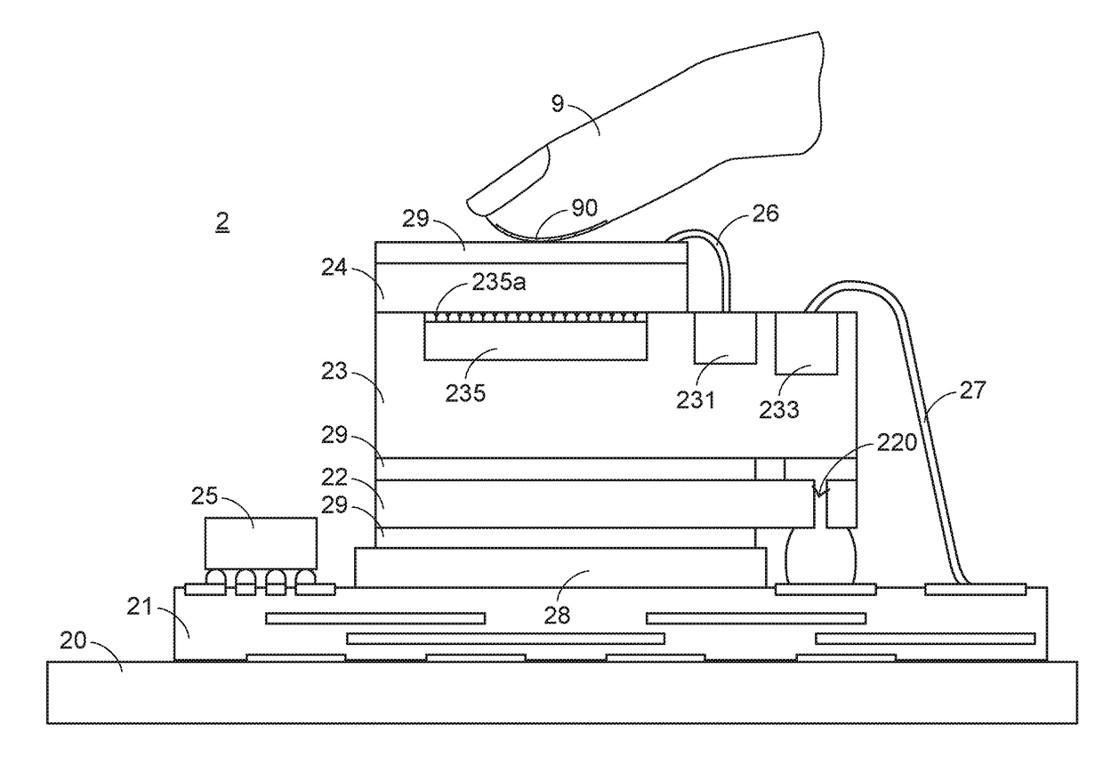
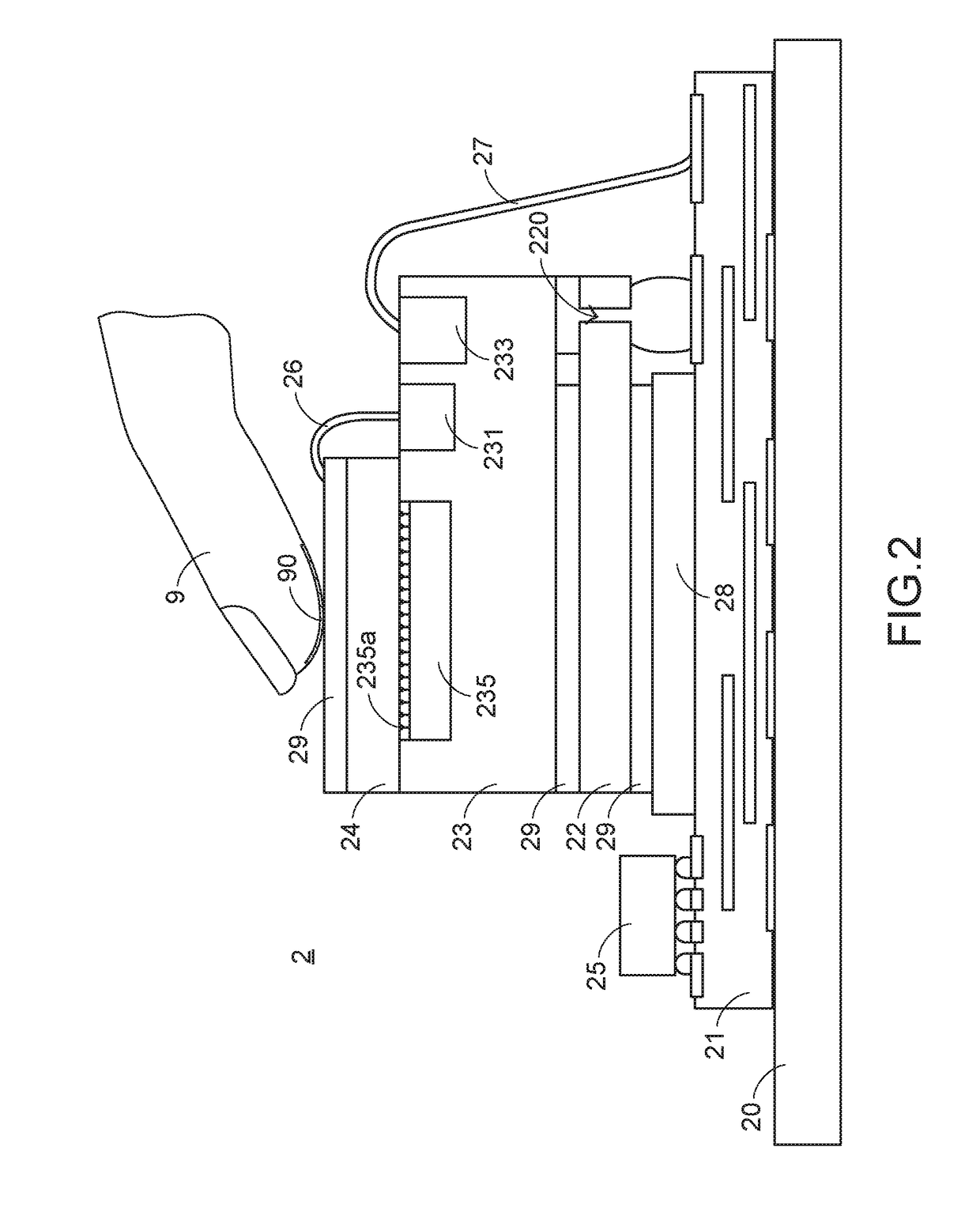
[0029]FIG. 2 is a schematic cross-sectional view illustrating an ultrasonic fingerprint recognition module according to a first embodiment of the present invention. As shown in FIG. 2, the ultrasonic fingerprint recognition module 2 comprises a substrate 21, an ultrasonic transmitter 22, a thin film transistor (TFT) 23, an ultrasonic receiver 24, a first wire 26 and a second wire 27. The above components will be described according to the sequence from bottom to top.

[0030]The substrate 21 is located at a bottom side. The ultrasonic transmitter 22 is stacked over the substrate 21. The thin film transistor 23 is stacked over the ultrasonic transmitter 22. The ultrasonic receiver 24 is stacked over the thin film transistor 23. The two ends of the first wire 26 are connected with the ultrasonic receiver 24 and a first electric pad 231 of the thin film transistor 23, respectively. Consequently, the ultrasonic receiver 24 and the thin film transistor 23 are electrically connected with each o


PUM


Abstract

An ultrasonic fingerprint recognition module and a manufacturing method thereof are provided. The ultrasonic fingerprint recognition module includes a substrate, an ultrasonic transmitter, a thin film transistor and an ultrasonic receiver. The method includes the following steps. In a step (a), the substrate, the ultrasonic transmitter, the thin film transistor and the ultrasonic receiver are provided. In a step (b), the ultrasonic transmitter is attached on a top surface of the substrate, and the ultrasonic transmitter is electrically connected with the substrate. In a step (c), the ultrasonic receiver is attached on the thin film transistor. In a step (d), the thin film transistor is attached on the ultrasonic transmitter. In a step (e), the ultrasonic receiver is electrically connected with the thin film transistor and the thin film transistor is electrically connected with the substrate through wires.

Description


Claims


Application Information

Patent Timeline
Owner PRIMAX ELECTRONICS LTD
Why Eureka
Try Eureka