Silicon carbide semiconductor device and method of manufacturing silicon carbide semiconductor device
a semiconductor device and silicon carbide technology, applied in the direction of semiconductor devices, basic electric elements, electrical equipment, etc., can solve the problems of forward characteristics degrading and the resistance of the nsup>/sup>-type drift layer increasing
- Summary
- Abstract
- Description
- Claims
- Application Information
AI Technical Summary
Benefits of technology
Problems solved by technology
Method used
Image

Examples
first embodiment
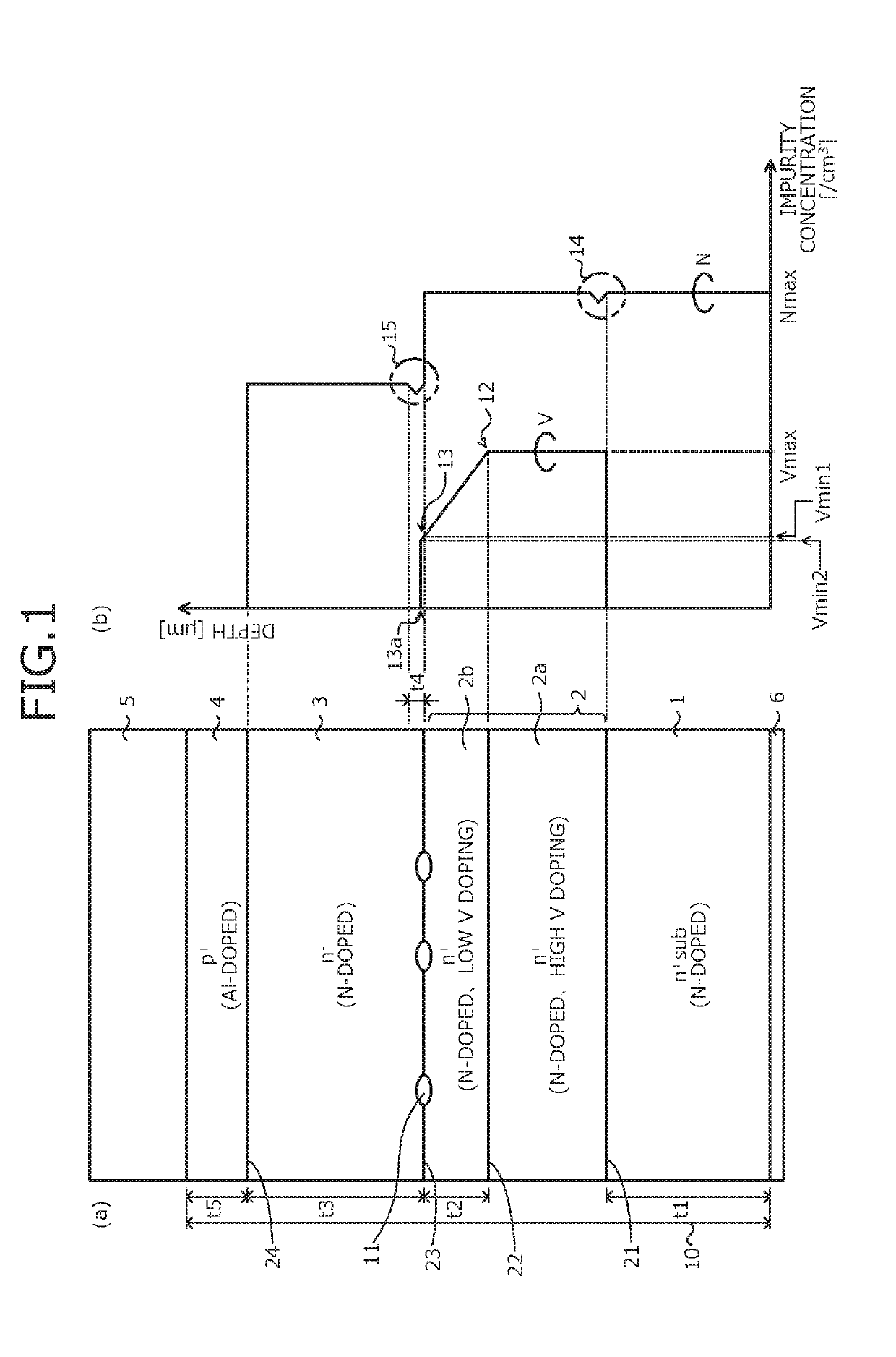
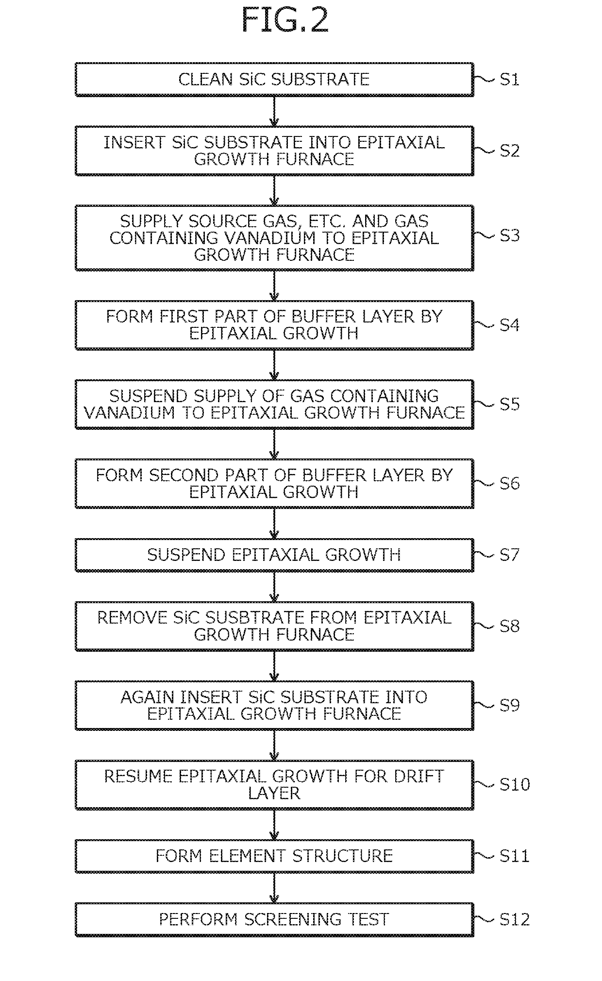
[0042]The silicon carbide semiconductor device depicted in FIG. 1 is a pin diode in which silicon carbide layers respectively constituting the n+-type buffer layer (or first first-conductivity-type epitaxial layer) 2, the n−-type drift layer 3, and the p+-type anode layer 4 are sequentially formed by epitaxial growth on a front surface of the n+-type starting substrate 1 that contains silicon carbide. An anode electrode 5 and a cathode electrode 6 are electrically connected to the p+-type anode layer 4 and a rear surface of the n+-type starting substrate 1 (or n+-type cathode layer), respectively.
[0043]For example, nitrogen (N) is introduced into the n+-type starting substrate 1 as an n-type dopant. An n-type impurity concentration (or nitrogen concentration) and a thickness t1 of the n+-type starting substrate 1, for example, may be about 5.0×10¹⁸ / cm3 and about 350 μm, respectively. In FIG. 1 and FIG. 3, introduction of nitrogen as a dopant is indicated as “N doped”.
[0044]The n+-ty
second embodiment
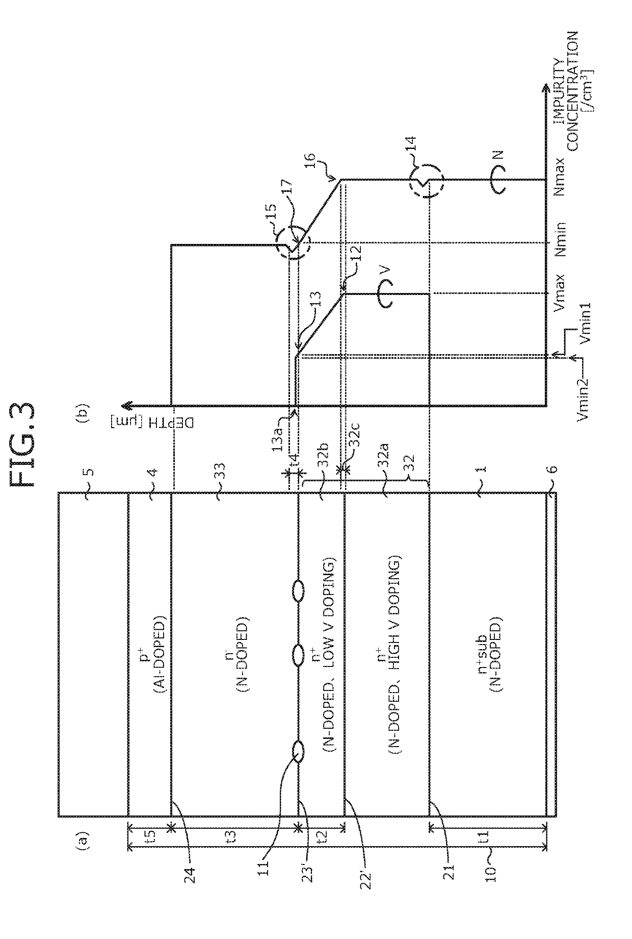
[0085]In the second embodiment, the n-type impurity concentration (or nitrogen concentration) in the n−-type drift layer 33 is set to be about 1×10¹⁵ / cm3 or less, thereby enabling high breakdown voltage. In particular, the n-type impurity concentration (or nitrogen concentration) and the thickness t3 of the n−-type drift layer 33, for example, may be set to be about 3×10¹⁴ / cm3 and about 150 μm, respectively, for a 13 kV pin diode. In this case, the n-type impurity concentration in the second part 32b of the n+-type buffer layer 32 is reduced, whereby auto-doping of the n-type impurity (or nitrogen) from the n+-type buffer layer 32 to the n−-type drift layer 33 at a high concentration may be suppressed during epitaxial growth of the n−-type drift layer 33.
[0086]The method of manufacturing a silicon carbide semiconductor device according to the second embodiment includes in the method of manufacturing a silicon carbide semiconductor device according to the first embodiment (refer to
PUM
 Abstract
Description
Claims
Application Information
 - R&D Engineer
- R&D Manager
- IP Professional
- Industry Leading Data Capabilities
- Powerful AI technology
- Patent DNA Extraction
Browse by: Latest US Patents, China's latest patents, Technical Efficacy Thesaurus, Application Domain, Technology Topic.
© 2024 PatSnap. All rights reserved.Legal|Privacy policy|Modern Slavery Act Transparency Statement|Sitemap