Semiconductor memory device
a memory device and semiconductor technology, applied in the direction of semiconductor devices, basic electric elements, electrical appliances, etc., can solve the problems of limited integration of 2d semiconductor devices, and achieve the effect of improving reliability
- Summary
- Abstract
- Description
- Claims
- Application Information
AI Technical Summary
Benefits of technology
Problems solved by technology
Method used
Image

Examples
Embodiment Construction
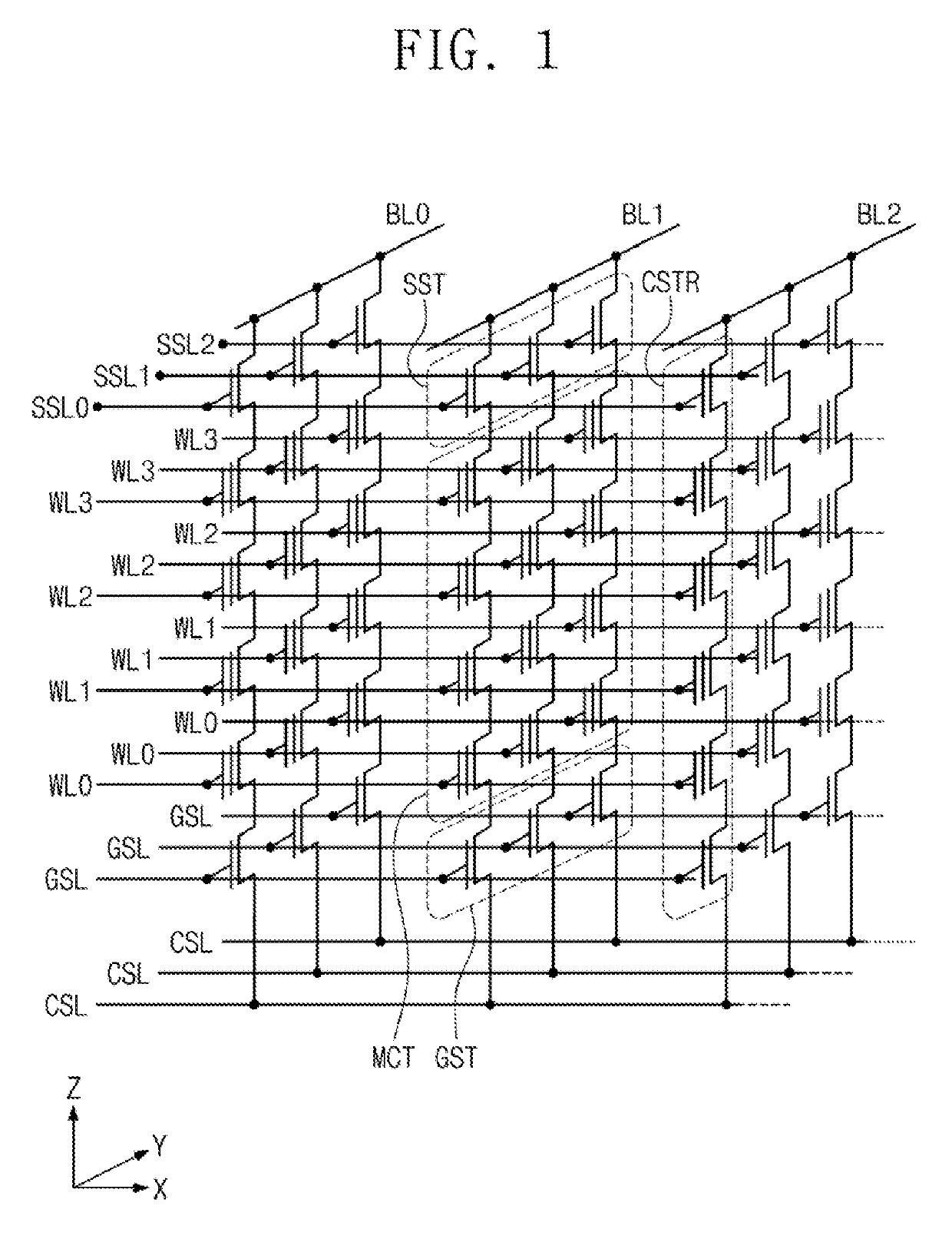
[0029]FIG. 1 is a schematic circuit diagram illustrating a cell array of a semiconductor memory device according to an exemplary embodiment of the present inventive concept.
[0030]Referring to FIG. 1, a semiconductor memory device may include a common source line CSL, a plurality of bit lines BL0 to BL2, and a plurality of cell strings CSTR provided between the common source line CSL and the plurality of bit lines BL0 to BL2.
[0031]The plurality of bit lines BL0 to BL2 may be two-dimensionally arranged and the plurality of cell strings CSTR may be connected in parallel to each of the plurality of bit lines BL0 to BL2 and connected to the common source line CSL. Thus, the cell strings CSTR may be two-dimensionally arranged on the common source line CSL or a substrate. The common source line CSL may be provided in plural, with the plurality of common source lines CSL supplied with the same voltage, or in some instances independently controlled and supplied with voltages different from each
PUM
 Abstract
Description
Claims
Application Information
 - R&D Engineer
- R&D Manager
- IP Professional
- Industry Leading Data Capabilities
- Powerful AI technology
- Patent DNA Extraction
Browse by: Latest US Patents, China's latest patents, Technical Efficacy Thesaurus, Application Domain, Technology Topic.
© 2024 PatSnap. All rights reserved.Legal|Privacy policy|Modern Slavery Act Transparency Statement|Sitemap