Method of forming a non-continuous conductive layer for laminated substrates

Inactive Publication Date: 2007-05-15
ROUND ROCK RES LLC
View PDF20 Cites 0 Cited by
  • Summary
  • Abstract
  • Description
  • Claims
  • Application Information

AI Technical Summary

Benefits of technology

[0009]A method for fabricating a circuit board having a non-continuous conductive layer is disclosed. A conductive layer is lamin

Problems solved by technology

Minor defects or deformations in these substrates or circuit boards can have a significant impact on further processing of the circuit board which includes attaching components, such as integrated circuits, to the circuit board.
Processing requires strict tolerances and even minor deformations can damage equipment or render a circ

Method used


Image

  • Method of forming a non-continuous conductive layer for laminated substrates
  • Method of forming a non-continuous conductive layer for laminated substrates
  • Method of forming a non-continuous conductive layer for laminated substrates

Examples


Embodiment Construction

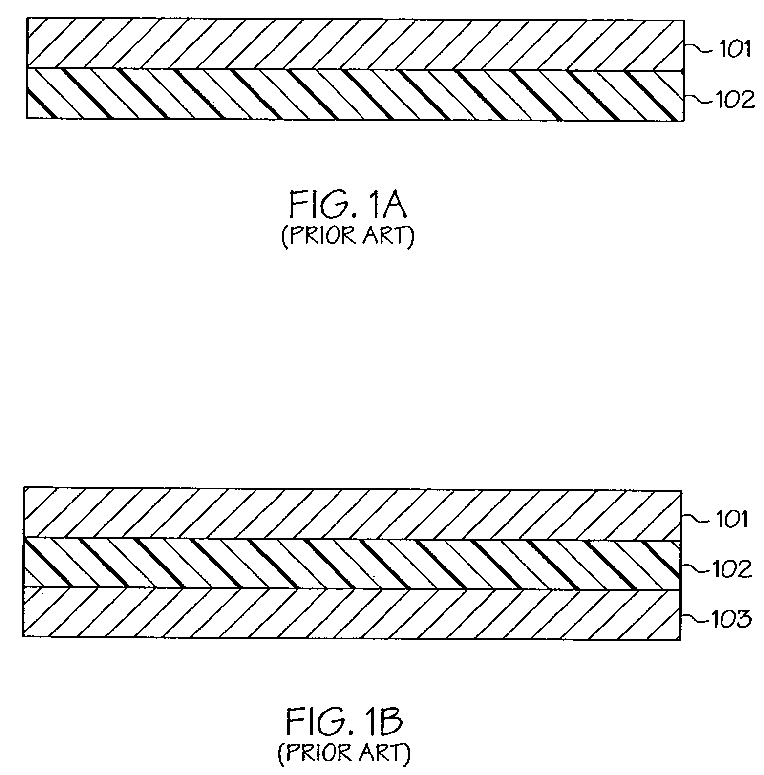
[0026]The term “patterning” refers to one or more steps that result in the removal of selected portions of layers. The patterning process is also known by the names photomasking, masking, photolithography and microlithography. The term “circuit board” refers to a flat piece of insulating material, such as epoxy or phenolic resin, on which electrical components are mounted and interconnected.

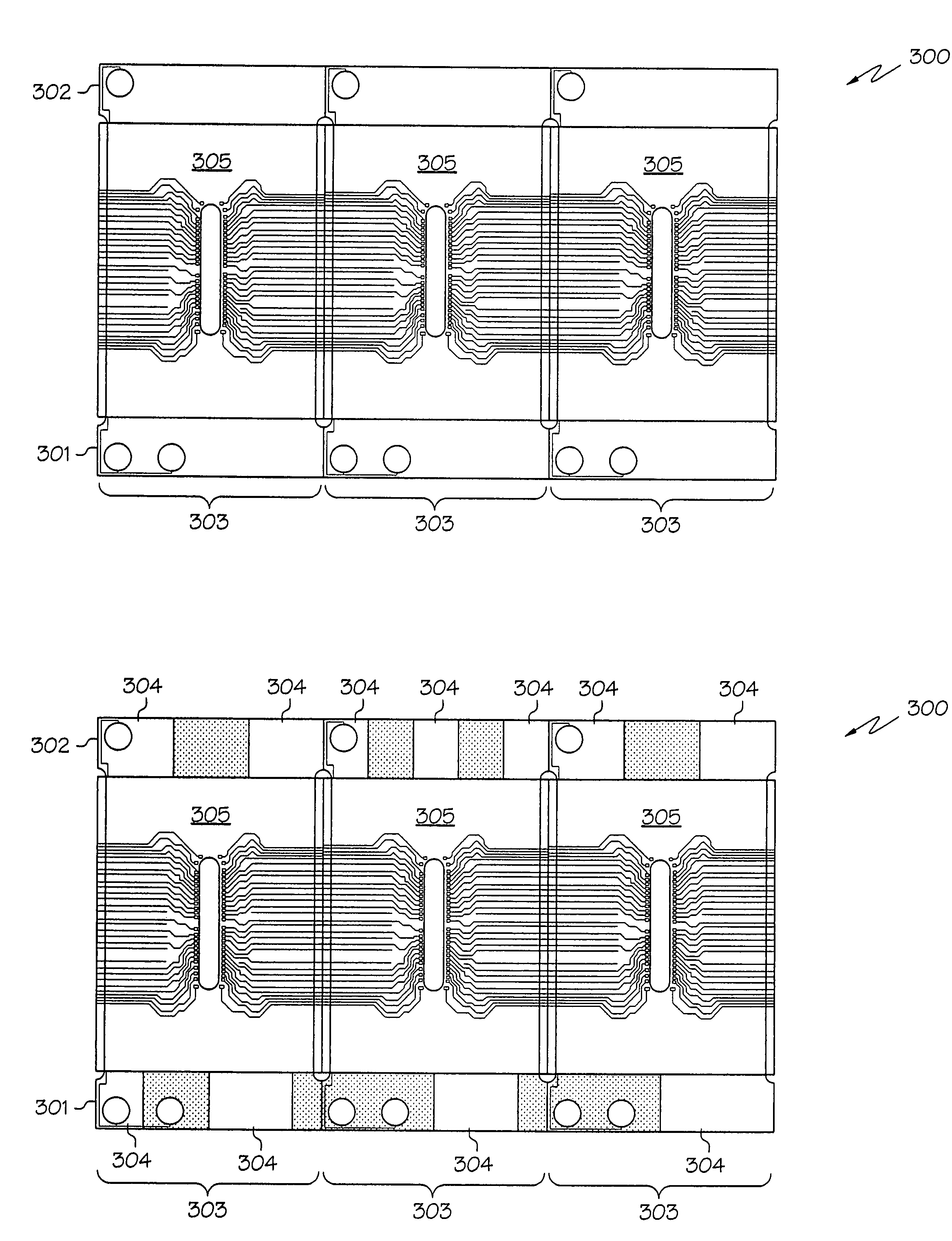
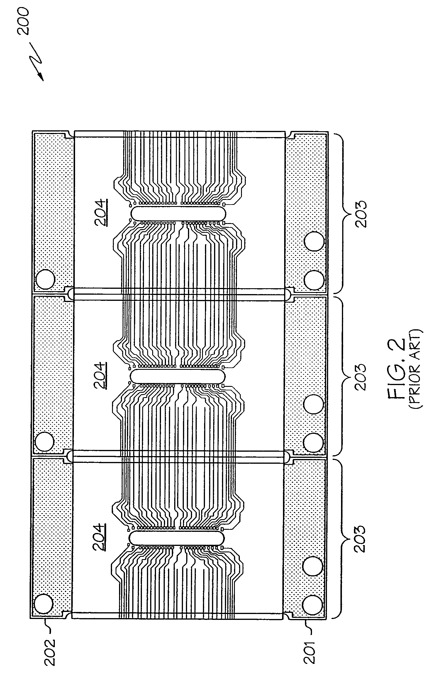
[0027]As stated earlier, FIG. 2 is an example of a standard circuit board 200 used for memory devices such as dual in line memory modules (DIMMs). The circuit board includes a first rail 201, a second rail 202, a number of sites 203 and a patterned area 204. A rail is an area along the edge of a circuit board. The rails 201 and 202 do not generally contain conductive paths, bonding pads or the like. Thus, the rails 201 and 202 do not get etched and conductive material is not removed from the rails 201 and 202. The rails 201 and 202 include a large amount of conductive material such as copper. The co


PUM

PropertyMeasurementUnit
Lengthaaaaaaaaaa
Electrical conductoraaaaaaaaaa

Abstract

A method of fabricating a circuit board is provided that includes forming a first layer of conductive material over an insulating layer, removing portions of the conductive material to define a first circuit pattern and a first rail area that is electrically isolated from the first circuit pattern, and removing portions of the conductive material from the first rail area. Optionally, the first rail area is positioned generally adjacent to a first edge of the circuit board and spans at least a portion of the length of the first edge. Optionally, portions of the conductive material of the first layer are removed to define a second rail area that is electrically isolated from the first circuit pattern and the first rail area, and portions of the conductive material of the first layer are also removed from the second rail area.

Description


Claims


Application Information

Patent Timeline
Owner ROUND ROCK RES LLC
Why Eureka
Try Eureka