Method for manufacturing a liquid crystal display
a liquid crystal display and manufacturing method technology, applied in the field of liquid crystal display manufacturing, can solve the problems of high manufacturing cost, complicated manufacturing process, low productivity, etc., and achieve the effects of sharply reducing manufacturing costs, reducing the number of photolithography processes, and improving manufacturing yield
- Summary
- Abstract
- Description
- Claims
- Application Information
AI Technical Summary
Benefits of technology
Problems solved by technology
Method used
Image

Examples
Embodiment Construction
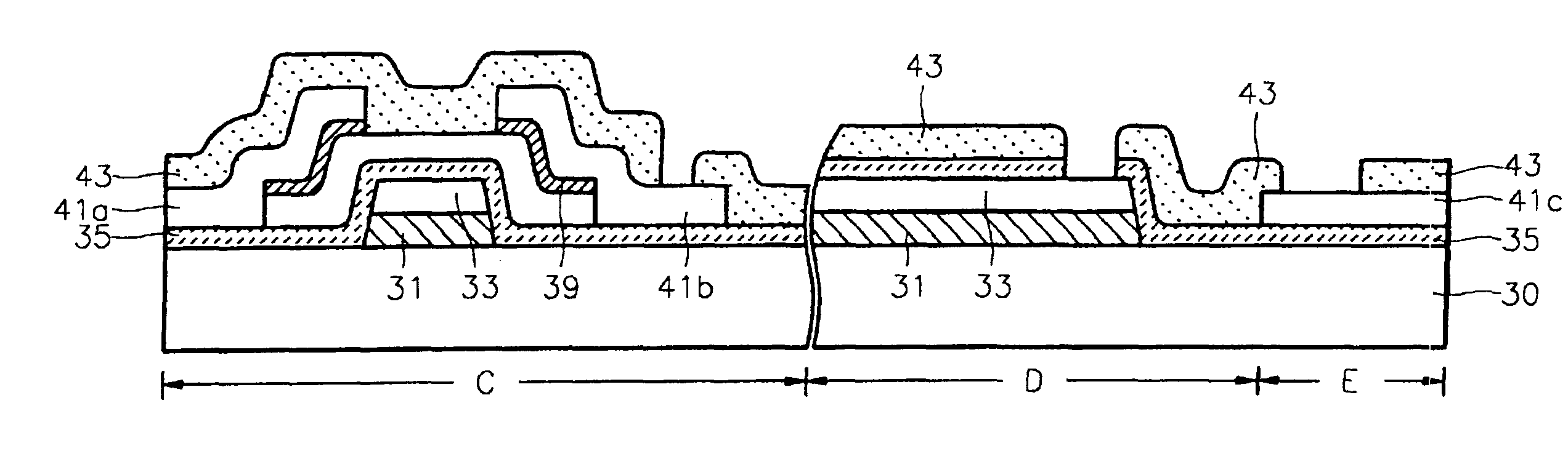
[0029]FIG. 6 is a schematic plan view of the mask patterns used for manufacturing a liquid crystal display according to the present invention, in which reference numeral 100 denotes a mask pattern for forming a gateline; reference numeral 105 denotes a mask pattern for forming a gate pad; reference numeral 110 denotes a mask pattern for forming a data line, reference numeral 115 denotes a mask pattern for forming a data pad; reference numeral 120 denotes a mask pattern for forming a semiconductor film; reference numeral 130 denotes a mask pattern for forming a source electrode / drain electrode; reference numeral 140 denotes a mask pattern for forming a contact hole for connecting a pixel electrode to the drain electrode in the TFT area; reference numeral 145 denotes a mask pattern for forming a contact hole for connecting a gate pad in the pad area to the pixel electrode; reference numeral 150 denotes a mask pattern for forming a pixel electrode in the TFT area; and reference numeral
PUM
 Abstract
Description
Claims
Application Information
 - R&D Engineer
- R&D Manager
- IP Professional
- Industry Leading Data Capabilities
- Powerful AI technology
- Patent DNA Extraction
Browse by: Latest US Patents, China's latest patents, Technical Efficacy Thesaurus, Application Domain, Technology Topic.
© 2024 PatSnap. All rights reserved.Legal|Privacy policy|Modern Slavery Act Transparency Statement|Sitemap