Packaging method of light-emitting or light-receiving diode
A technology of photodiode and packaging method, which is applied in the direction of electrical components, electric solid-state devices, circuits, etc., can solve the problems of difficult heat conduction function and high cost, and achieve the effect of improving heat conduction function and reducing the packaging volume
- Summary
- Abstract
- Description
- Claims
- Application Information
AI Technical Summary
Benefits of technology
Problems solved by technology
Method used
Image

Examples
Embodiment Construction
[0012] The embodiments of the present invention will be described in more detail below with reference to the drawings and component symbols, so that those skilled in the art can implement them after studying this specification.
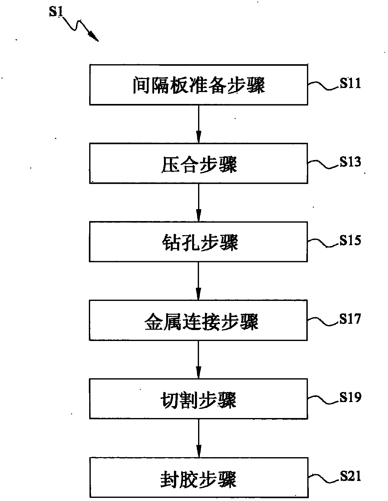
[0013] refer to figure 1 , a flow chart of the packaging method of the light-emitting or light-receiving diode of the present invention. The packaging method S1 of the light-emitting or light-receiving diode of the present invention includes: a spacer plate preparation step S11, a pressing step S13, a drilling step S15, a metal connection step S17, a cutting step S19, and a sealing step S21.
[0014] The spacer plate preparation step S11 is to prepare a spacer plate, and the spacer plate has a plurality of crystal die cavities, each of which is used to carry and accommodate at least one light-emitting or light-receiving diode die; the pressing step S13 is to combine multiple The light-emitting or light-receiving diode die is placed in the die cavity, an
PUM
 Abstract
Description
Claims
Application Information
 - R&D Engineer
- R&D Manager
- IP Professional
- Industry Leading Data Capabilities
- Powerful AI technology
- Patent DNA Extraction
Browse by: Latest US Patents, China's latest patents, Technical Efficacy Thesaurus, Application Domain, Technology Topic.
© 2024 PatSnap. All rights reserved.Legal|Privacy policy|Modern Slavery Act Transparency Statement|Sitemap