Printed circuit board and preparation method thereof

A technology for printed circuit boards and substrates, used in multilayer circuit manufacturing, printed circuit components, etc., can solve the problems of difficult to control impedance, uneven thickness of media, etc., to improve consistency, uniform thickness of media, and reduce expansion and contraction. sexual effect

Inactive Publication Date: 2014-11-19
SHENZHEN SUNTAK MULTILAYER PCB
View PDF4 Cites 6 Cited by
  • Summary
  • Abstract
  • Description
  • Claims
  • Application Information

AI Technical Summary

Problems solved by technology

[0003] The technical problem to be solved by the present invention is to provide a solution between the outer layer copper foil and the inner layer circuit in order to solve the problem that the impedance is difficult to control due to the uneven thickness of the me...

Method used


Image

  • Printed circuit board and preparation method thereof
  • Printed circuit board and preparation method thereof

Examples


Embodiment

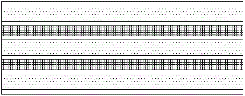
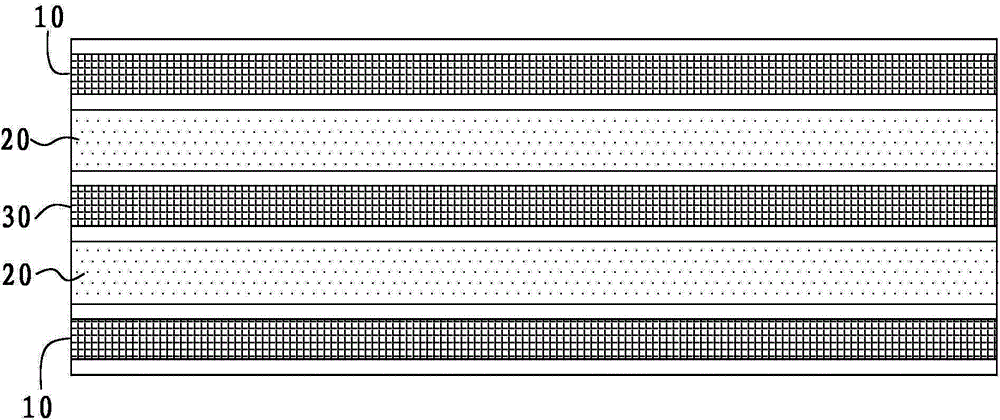
[0019] refer to figure 2 , a multilayer printed circuit board provided in this embodiment includes two outer layer boards 10, an inner layer board 30 and a prepreg 20 as a bonding material, and according to the outer layer board 10, the prepreg 20, the inner layer board 30, The prepreg 20 and the outer layer board 10 are laminated and bonded in sequence to form a six-layer printed circuit board. The inner board 30 is a substrate with inner circuit patterns on both surfaces; the outer board 10 is a substrate with inner circuit patterns on one surface and outer circuit patterns on the other surface. The side of the outer layer board 10 with the outer layer circuit pattern is used as the outer surface of the multilayer printed circuit board, that is, the surfaces of the two outer layer boards 10 with the inner layer circuit pattern face each other.

[0020] The preparation method of the multilayer printed circuit board of the present embodiment comprises the following steps:

...


PUM


Abstract

The invention relates to the technical field of circuit board production, in particular to a multilayer printed circuit board and a preparation method thereof. The multilayer printed circuit board comprises two outer layer boards and prepregs, wherein the two outer layer boards are integrally pressed through the prepregs; an inner layer route pattern is arranged on one surface of each outer layer board, and a baseplate with an outer layer route pattern is arranged on the other surface of each outer layer board; the multilayer printed circuit board is prepared from the procedures of board cutting, inner layer pattern transferring, pressing, outer layer pattern transferring and the like in sequence. By the adoption of the outer layer boards with the inner layer patterns on one surfaces and integral copper-clad surfaces on the other surfaces to form an outer layer copper foil of the multilayer printed circuit board, the media between the outer layer copper foil and a secondary outer layer copper foil are uniform in thickness, the influence of the media on the outer layer of the multilayer printed circuit board on the impedance can be steadily controlled, and uniformity of the impedance in different regions of the same large board is improved; the structural features of the multilayer printed circuit board are matched with the specific pressing process parameters to reduce the swell-shrink characteristic of the multilayer printed circuit board.

Description

technical field [0001] The invention relates to the technical field of printed circuit boards, in particular to a printed circuit board and a preparation method thereof. Background technique [0002] The printed circuit board is the support of electronic components and provides electrical connections for electronic components. Multilayer printed circuit boards are usually made by pressing the etched copper clad laminate, outer copper foil and prepreg, and the outer copper foil is bonded to the etched copper clad laminate and the lower surface (such as figure 1 shown); by changing the number of etched copper clad laminates between the two outer layers of copper foil, printed circuit boards with different number of circuit layers can be obtained. Therefore, the upper and lower surfaces of the existing multilayer printed circuit board are the outer layer copper foil bonded by the prepreg and the pressing process, and the outer layer copper foil and the copper foil on the adjac...

Claims


Application Information

Patent Timeline
Patent Type & Authority Applications(China)
IPC IPC(8): H05K1/02H05K3/46
Inventor 赵波刘东翟青霞王佐
Owner SHENZHEN SUNTAK MULTILAYER PCB
Why Eureka
Try Eureka