Array substrate, display panel and preparation method of array substrate

A technology for array substrates and display panels, applied in semiconductor/solid-state device manufacturing, semiconductor devices, electrical components, etc., can solve problems such as electrode signal interruption, film layer shedding, etc., to avoid electrode signal interruption, reduce step difference, reduce The effect of the risk of shedding

Active Publication Date: 2017-05-24
BOE TECH GRP CO LTD +1
View PDF4 Cites 4 Cited by
  • Summary
  • Abstract
  • Description
  • Claims
  • Application Information

AI Technical Summary

Problems solved by technology

[0005] Aiming at the above-mentioned deficiencies in the prior art, the present invention provides an array substrate, a display panel, and a method for preparing the array substrate, so as to solve the problem of electrode signal interruption caused by the peeling off of the film layer at the position of the via hole

Method used


Image

  • Array substrate, display panel and preparation method of array substrate
  • Array substrate, display panel and preparation method of array substrate
  • Array substrate, display panel and preparation method of array substrate

Examples


Embodiment Construction

[0041] The technical solutions in the present invention will be clearly and completely described below in conjunction with the accompanying drawings in the present invention. Apparently, the described embodiments are part of the embodiments of the present invention, not all of them. Based on the embodiments of the present invention, all other embodiments obtained by persons of ordinary skill in the art without making creative efforts belong to the protection scope of the present invention.

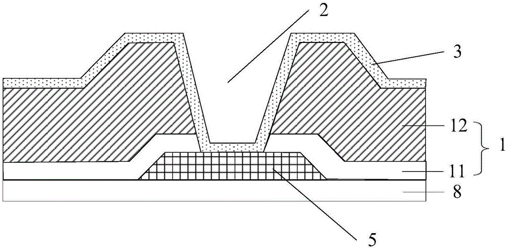
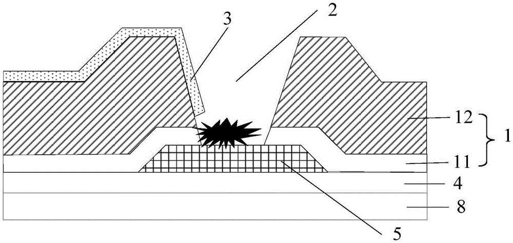
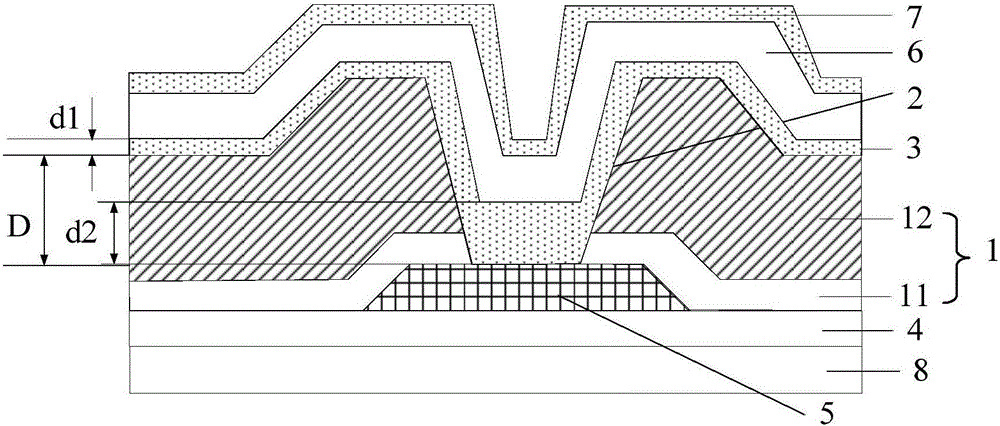
[0042] Combine the following figure 2 , detailing the structure of the array substrate of the present invention.

[0043] Such as figure 2 As shown, the present invention provides an array substrate, including a substrate 8 , a protective layer 1 formed on the substrate 8 , and a via hole 2 penetrating through the protective layer 1 . The array substrate further includes a first conductive layer 3, the first conductive layer 3 is located on the side away from the substrate 8 on the pro...


PUM


Abstract

The invention provides an array substrate, a display panel and a preparation method of the array substrate. The array substrate comprises a protective layer and a through hole and also comprises a first conducting layer, wherein the protective layer is formed on the substrate; the through hole penetrates through the protective layer; the first conducting layer is positioned on one side, far away from the substrate, of the protective layer with the through hole. The thickness of the first conducting layer at the bottom part of the through hole is more than that of the first conducting layer at the area beyond the through hole, namely, the thickness of the first conducting layer at the bottom part of the through hole is increased, and the section difference between the bottom of a middle hole and the top of the hole can be reduced, so that the risk of dropping of the first conducting film layer in the through hole is reduced, further the signal interruption of the electrodes is avoided and the electric connection performance of a TFT (Thin Film Transistor) is improved.

Description

technical field [0001] The invention relates to the field of display technology, in particular to an array substrate, a display panel and a method for preparing the array substrate. Background technique [0002] see Figure 1a , the existing TFT (Thin Film Transistor, thin film transistor) includes: a buffer layer 4, a signal line 5, and a protective layer 1 (including a first protective layer 11 and a second protective layer 12) formed on a substrate 8 in sequence. A via hole 2 penetrating through the protection layer 1 is formed at the position of the signal line area on the layer 1 , and the first conductive layer 3 is connected to the signal line 5 through the via hole 2 . [0003] The thickness of the second protective layer 12 is about 10000A-20000A (current production standard, non-industry standard), and the thickness of the first conductive layer 3 formed on the second protective layer 12 is about 400A (current production standard, non-industry standard) , the film...

Claims


Application Information

Patent Timeline
IPC IPC(8): H01L27/12H01L21/77
CPCH01L21/77H01L27/12H01L27/1214H01L27/124H01L27/1244H01L27/1259H01L2021/775
Inventor 肖志莲蒋会刚裴晓光刘冲赵海生黄雄天肖红玺
Owner BOE TECH GRP CO LTD
Why Eureka
Try Eureka