Manufacturing method of flexible electronic device based on LIG
A flexible electronic device and manufacturing method technology, applied in the direction of instrument, electrical digital data processing, data processing input/output process, etc., can solve the problems of unfavorable laser-induced graphene industrialization, difficult operation of screen printing silver paste, graphite The mechanical properties of the olefin pattern layer are weak and other problems, so as to reduce the production cost, ensure the processing efficiency, and improve the conductivity.
- Summary
- Abstract
- Description
- Claims
- Application Information
AI Technical Summary
Problems solved by technology
Method used
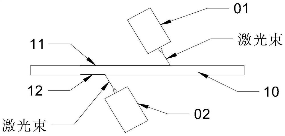
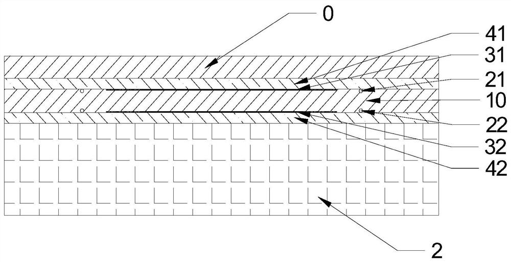
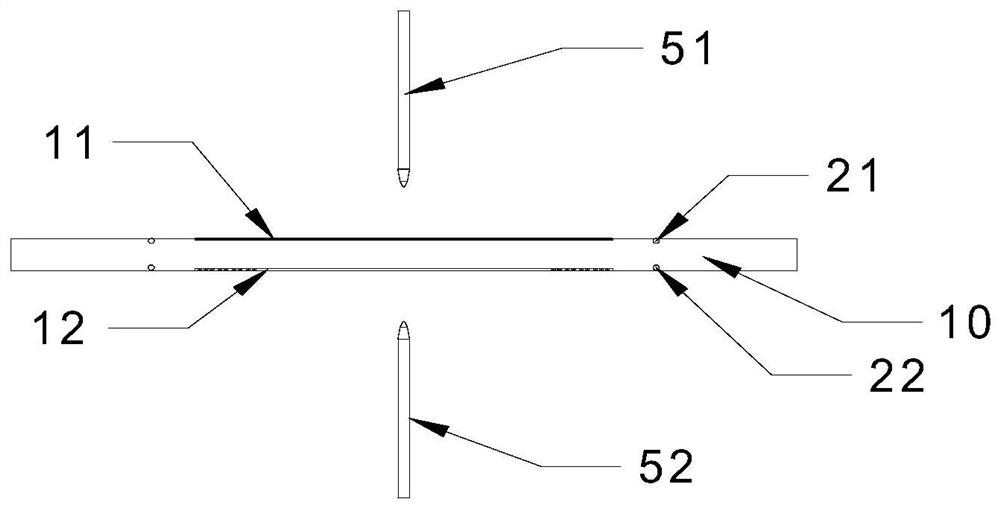
Image

Examples
Example Embodiment
[0031] Hereinafter, some exemplary embodiments are simply described. As will be appreciated by those skilled in the art, the described embodiments can be modified in a variety of different ways without departing from the spirit or scope of the invention. Thus, the drawings and descriptions are considered to be exemplary rather than restrictive.
[0032] In the description of the present invention, it is to be understood that the term * # * center * # * * # * longitudinal * # * * # * Cross * # * * # * length * # * * # * width * # * * # * thickness * # * * # * a * # * * # * the * # * * # * before * # * * # * after * # * * # * left * # * * # * Right * # * * # * kin straight * # * * # * level * # * * # * top * # * * # * bottom * # * * # * inside * # *, orientation or positional relationship of the outer * # * # * * # * # * * * clockwise, counterclockwise * # * # * etc. * indicates the position or orientation of the relationship shown in the accompanying drawings, this is merely for conve
PUM
| Property | Measurement | Unit |
|---|---|---|
| Wavelength | aaaaa | aaaaa |
Abstract
Description
Claims
Application Information
 - R&D Engineer
- R&D Manager
- IP Professional
- Industry Leading Data Capabilities
- Powerful AI technology
- Patent DNA Extraction
Browse by: Latest US Patents, China's latest patents, Technical Efficacy Thesaurus, Application Domain, Technology Topic.
© 2024 PatSnap. All rights reserved.Legal|Privacy policy|Modern Slavery Act Transparency Statement|Sitemap