Nano-copper soldering paste and application thereof in chip packaging interconnection structure
A technology of nano-copper and solder paste, which is applied in the direction of welding medium, welding equipment, welding/cutting medium/material, etc., can solve the problems of low cost and oxidation of nano-copper solder paste, and achieve reduced production costs, prevention of oxidation, and high melting point Effect
- Summary
- Abstract
- Description
- Claims
- Application Information
AI Technical Summary
Problems solved by technology
Method used
Image

Examples
Example Embodiment
[0041] Example 1
[0042] Embodiments of the present invention provide a nano-copper solder paste that includes nano-copper particles, reducing agents, and an organic solvent carrier mixed with each other.
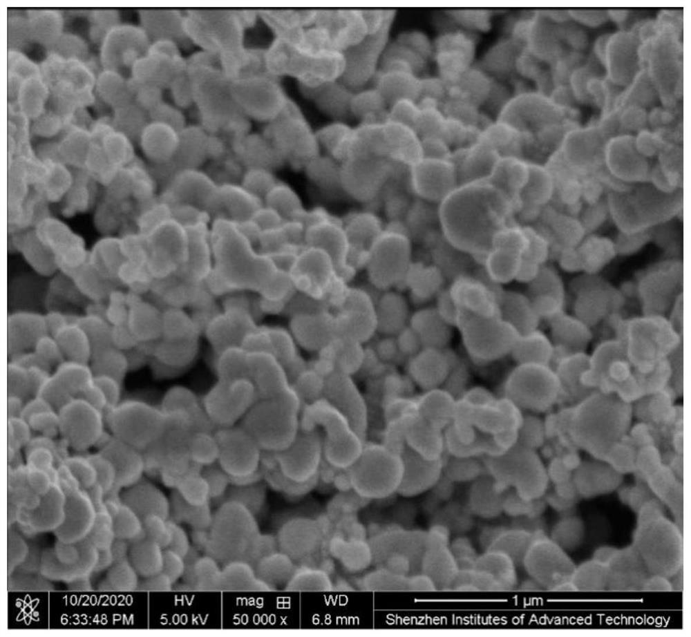
[0043] Among them, the nanoplasm particles select spherical nano-copper particles having a particle diameter of 50 nm to 300 nm, and the SEM map of the spherical nano-copper particles in this example is figure 2 As shown; the reducing agent is selected as an ascorbic acid; the organic solvent carrier is selected as a mixture of glycerol and β-terpinol alcohol mass of 1: 1.
[0044] Among them, in this embodiment, the mass ratio of the nanocoprus particles, reducing agents, and the organic solvent carrier is 6: 0.5: 1. According to the above mass ratio, the nanoplasm particles, reducing agents, and organic solvent carriers were stirred and mixed, and the nano-copper solder paste was obtained.
[0045] The above-prepared nano-copper solder paste is applied to the package interconne
Example Embodiment
[0051] Example 2
[0052] Embodiments of the present invention provide a nano-copper solder paste that includes nano-copper particles, reducing agents, and an organic solvent carrier mixed with each other.
[0053] Among them, the nano-copper particles select a spherical nano-copper particles having a particle diameter of 50 nm to 300 nm, and the reducing agent is selected as a citrate; the organic solvent carrier is selected to be ethylene glycol and γ-terpene alcohol mass ratio of 1: 1 mixture.
[0054] Among them, in this example, the mass ratio of the nanocoprus particles, reducing agents, and the organic solvent carrier is 5: 0.3: 1. According to the above mass ratio, the nanoplasm particles, reducing agents, and organic solvent carriers were stirred and mixed, and the nano-copper solder paste was obtained.
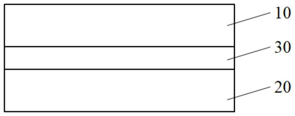
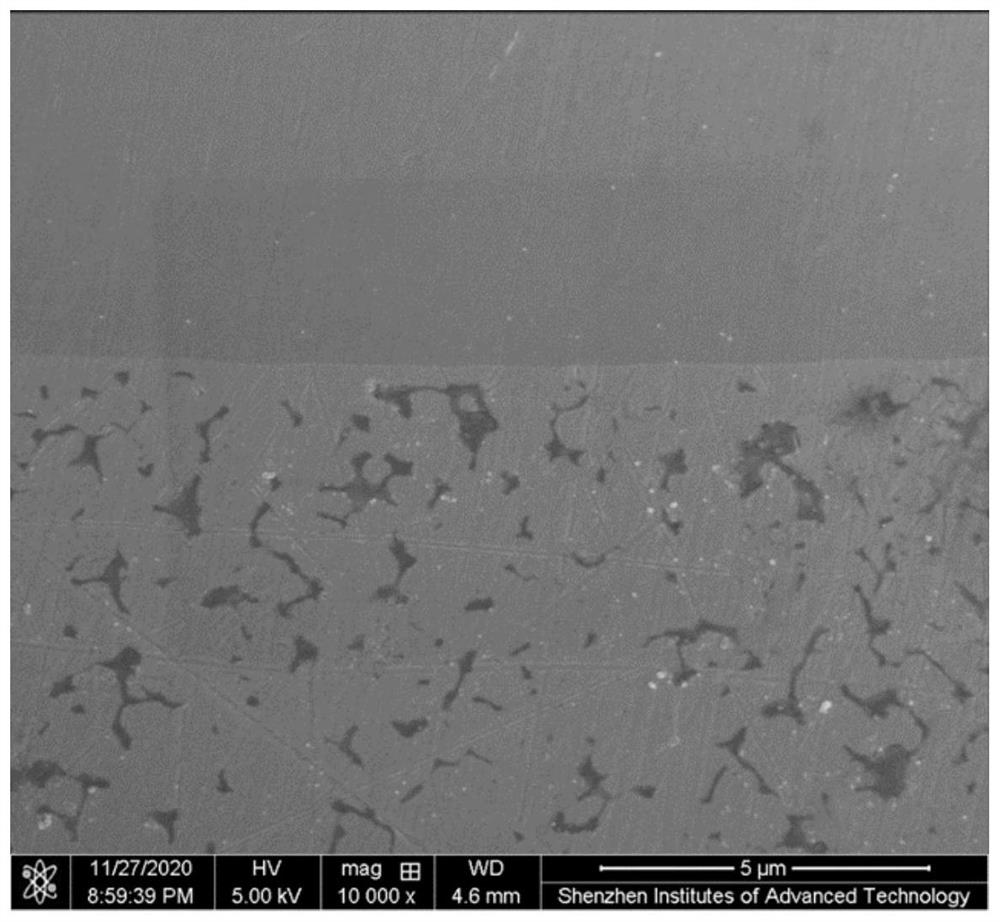
[0055] The above-prepared nano-copper solder paste is applied to the package interconnection of the electronic device. Specifically, see figure 1 The first mother and the s
Example Embodiment
[0060] Example 3
[0061] Embodiments of the present invention provide a nano-copper solder paste that includes nano-copper particles, reducing agents, and an organic solvent carrier mixed with each other.
[0062] Among them, the nano-copper particles select spheroid nanoplasia particles having a particle diameter of 50 nm to 300 nm; the reducing agent is selected to be sodium borohydride; the organic solvent carrier is selected to be a mixture of ethylene glycol and diethylene glycol according to a mass ratio of 1: 1.
[0063] In this embodiment, the mass ratio of the nanocoprus particles, reducing agents, and the organic solvent carrier is 4: 0.2: 1. According to the above mass ratio, the nanoplasm particles, reducing agents, and organic solvent carriers were stirred and mixed, and the nano-copper solder paste was obtained.
[0064] The above-prepared nano-copper solder paste is applied to the package interconnection of the electronic device. Specifically, see figure 1 The first m
PUM
| Property | Measurement | Unit |
|---|---|---|
| Particle size | aaaaa | aaaaa |
| Shear force | aaaaa | aaaaa |
| Shear force | aaaaa | aaaaa |
Abstract
Description
Claims
Application Information
 - R&D Engineer
- R&D Manager
- IP Professional
- Industry Leading Data Capabilities
- Powerful AI technology
- Patent DNA Extraction
Browse by: Latest US Patents, China's latest patents, Technical Efficacy Thesaurus, Application Domain, Technology Topic.
© 2024 PatSnap. All rights reserved.Legal|Privacy policy|Modern Slavery Act Transparency Statement|Sitemap