Semiconductor structure and semiconductor device
A semiconductor and device technology, applied in the field of semiconductor structures and semiconductor devices, to prevent the effect of affecting the test effect
- Summary
- Abstract
- Description
- Claims
- Application Information
AI Technical Summary
Benefits of technology
Problems solved by technology
Method used
Image

Examples
Embodiment 1
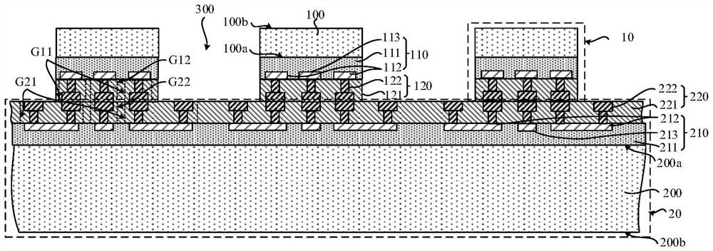
[0041] figure 1 This is a schematic structural diagram of the semiconductor structure provided in this embodiment. like figure 1 As shown, the semiconductor structure includes a plurality of first chips 10 and a wafer 20, the first chips 10 are bonded on the surface of the wafer 20 by hybrid bonding, and the first chips 10 and the The wafers 20 may be bonded together face-to-face.
[0042]Further, there is a gap 300 between two adjacent first chips 10 , the wafer 20 has a dicing area (not shown) for forming a dicing line, and the gap 300 is aligned and exposed The cutting area is subsequently cut through the cutting area on the wafer 20 to cut the semiconductor structure into individual bonding sheets, one bonding sheet corresponding to a second chip on the wafer 20 and a For the first chip 10, a semiconductor device can be formed after the bonding sheet is packaged. figure 1 Only three of the first chips 10 are schematically shown in the figure, and the gaps 300 between two
Embodiment 2
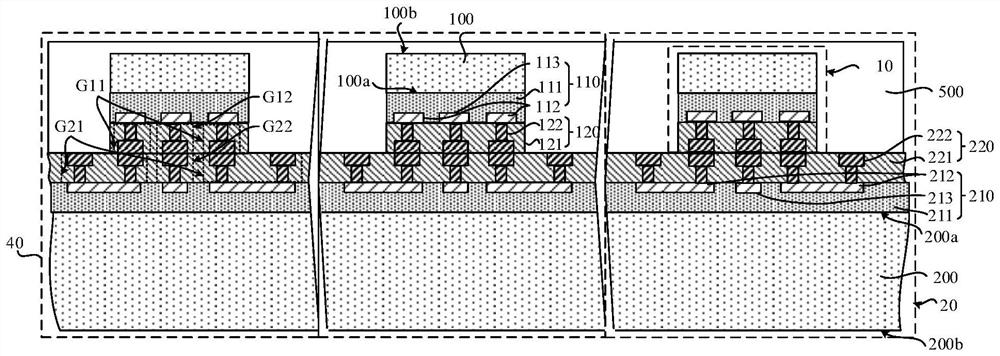
[0079] Figure 4 This is a schematic structural diagram of the semiconductor structure provided in this embodiment. like Figure 4 As shown, the difference from the first embodiment is that in this embodiment, the first interconnection structure layer has two, which are the first interconnection structure layer 110a and the first interconnection structure layer 110b respectively. Specifically, the first interconnect structure layer 110a is located on the first surface 100a of the first substrate 100 and covers the first surface 100a of the first substrate 100, and the first interconnect structure layer 110b is connected to the first surface 100a of the first substrate 100. The first hybrid bonding layer 120 is sequentially formed on the second surface 100b of the first substrate 100 and covers the second surface 100b of the first substrate 100, image 3 , the first interconnect structure layer 110a, the first substrate 100, the first interconnect structure layer 110b, and the f
PUM
 Abstract
Description
Claims
Application Information
 - R&D Engineer
- R&D Manager
- IP Professional
- Industry Leading Data Capabilities
- Powerful AI technology
- Patent DNA Extraction
Browse by: Latest US Patents, China's latest patents, Technical Efficacy Thesaurus, Application Domain, Technology Topic.
© 2024 PatSnap. All rights reserved.Legal|Privacy policy|Modern Slavery Act Transparency Statement|Sitemap