High-reliability low-defect semiconductor light-emitting device and preparation method thereof
A technology for light-emitting devices and semiconductors, which is applied to semiconductor lasers, laser components, structures of optical waveguide semiconductors, etc., can solve the problems of high process control cost, difficulty in taking into account reliability, etc., and achieves reduced technical difficulty, reduced optical catastrophe damage, Reduce the effect of coating shading
- Summary
- Abstract
- Description
- Claims
- Application Information
AI Technical Summary
Problems solved by technology
Method used
Image

Examples
Embodiment 1
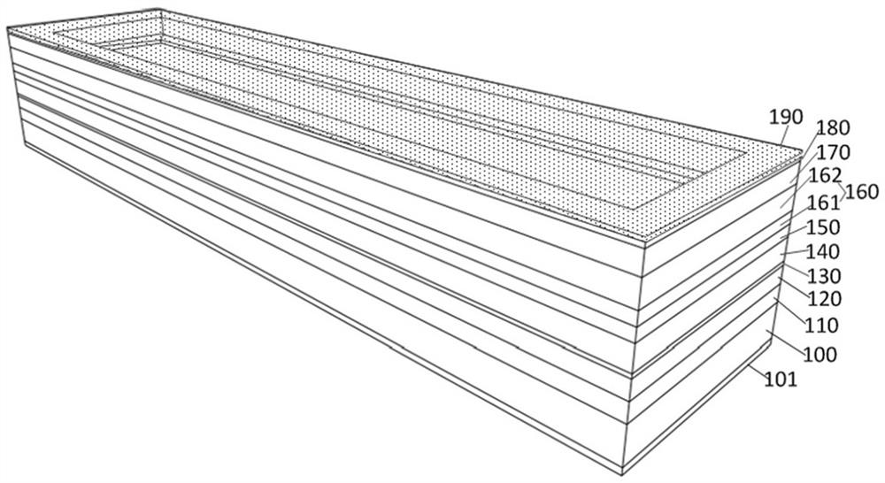
[0042] An embodiment of the present invention provides a high-reliability and low-defect semiconductor light-emitting device, refer to figure 1 ,include:
[0043] Semiconductor substrate layer 100;
[0044] an active layer 130 located on the semiconductor substrate layer;
[0045] A doped semiconductor contact layer 160 located on a side of the active layer 130 away from the semiconductor substrate layer 100, the doped semiconductor contact layer 160 comprising a first region and an edge region surrounding the first region;
[0046] a protection layer 170 located on a side of the edge region of the doped semiconductor contact layer 160 away from the active layer 130;
[0047] The front electrode layer 190 is located on the side of the first region away from the active layer 130 , and the upper surface of the front electrode layer 190 on the first region is lower than the upper surface of the protective layer 170 .
[0048] In this embodiment, the protective layer 170 is used t
Embodiment 2
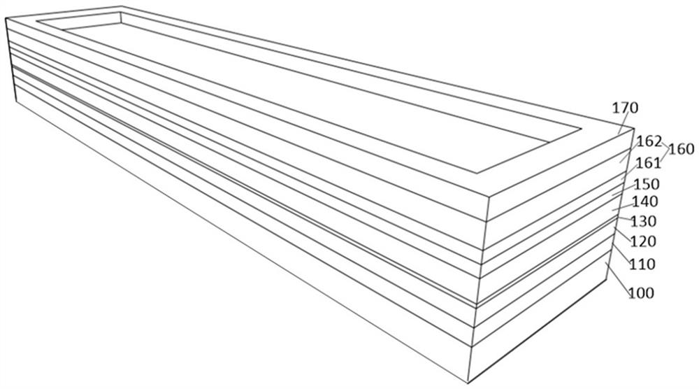
[0075] This embodiment provides a method for manufacturing a high-reliability and low-defect semiconductor light-emitting device. Refer to figure 1 ,include:
[0076] S1: providing a semiconductor substrate layer;
[0077] S2: forming an active layer on the semiconductor substrate layer;
[0078] S3: forming a doped semiconductor contact layer on a side of the active layer away from the semiconductor substrate layer, the doped semiconductor contact layer including a first region and an edge region surrounding the first region;
[0079] S4: forming a protective layer on the side of the edge region of the doped semiconductor contact layer away from the active layer;
[0080] S5: forming a front electrode layer on a side of the first region away from the active layer, the upper surface of the front electrode layer on the first region is lower than the upper surface of the protective layer.
[0081] refer to figure 2 , providing a semiconductor substrate layer 100; forming a low
PUM
| Property | Measurement | Unit |
|---|---|---|
| Thickness | aaaaa | aaaaa |
Abstract
Description
Claims
Application Information
 - R&D Engineer
- R&D Manager
- IP Professional
- Industry Leading Data Capabilities
- Powerful AI technology
- Patent DNA Extraction
Browse by: Latest US Patents, China's latest patents, Technical Efficacy Thesaurus, Application Domain, Technology Topic.
© 2024 PatSnap. All rights reserved.Legal|Privacy policy|Modern Slavery Act Transparency Statement|Sitemap