High power LED array module

A technology of light-emitting diodes and array modules, which is applied to semiconductor/solid-state device components, semiconductor devices, electrical components, etc., can solve the problems of poor luminous effect, reduced luminous efficiency, and small surface area of ​​array modules, so as to improve heat dissipation efficiency and Optical coupling performance, simplified packaging process, and improved power output

Inactive Publication Date: 2006-04-12
OPTO TECH
View PDF0 Cites 7 Cited by
  • Summary
  • Abstract
  • Description
  • Claims
  • Application Information

AI Technical Summary

Problems solved by technology

[0006] Another problem with assembly to form high power LED array modules is poor heat dissipation
A single packaged high-power light-emitting diode has a small surface area, so when used alone, it is easy to reduce the luminous efficiency due to high temperature
When it is assembled into an array module, the problem of poor heat dissipation will be more serious, resulting in poor luminous effect of the entire array module

Method used


Image

  • High power LED array module
  • High power LED array module
  • High power LED array module

Examples


Embodiment Construction

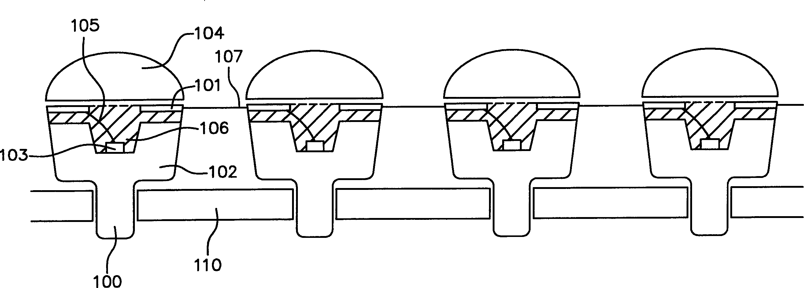
[0036] The high-power light-emitting diode array module of the present invention uses a circuit board with a plurality of placement holes to directly place high-power light-emitting diode chips into the placement holes for packaging. In this way, the volume of the array module can be greatly reduced. By configuring the heat dissipation structure in the circuit board, the heat dissipation efficiency can be significantly improved. Additionally, the lens on each placement hole can be adjusted for the array module to optimize the beam output.

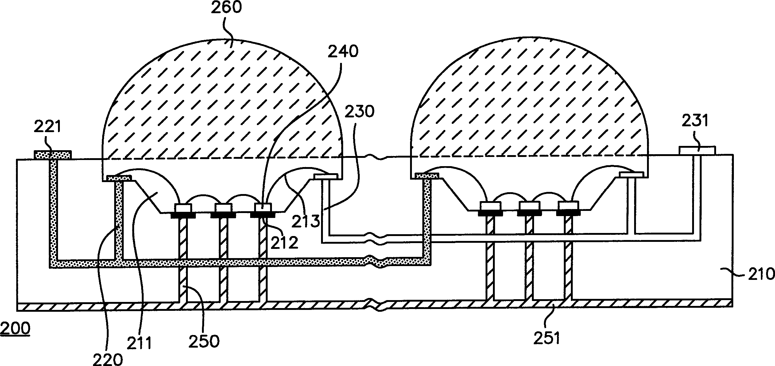
[0037] figure 2 It is a cross-sectional view of the high-power light-emitting diode array module in the first preferred embodiment of the present invention. The high-power LED array module 200 of the present invention includes a circuit board 210 , an anode 220 , a cathode 230 , a high-power LED chip 240 , a heat dissipation structure 250 , and a lens 260 .

[0038] The circuit board 210 has a plurality of placement holes 211 arranged i...


PUM


Abstract

This invention relates to a high power LED array module including a CB, multiple anodes and cathodes, multiple chips, a package material and multiple lenses, among which, the CB has many holes for putting the arrays, each hole has a cathode and an anode, the anodes in the holes are connected with each other and cathodes are connected with each other, each hole has at least a chip serial or parallel to the anode and the cathode in the hole, the package material fills the holes for fixing the chips and each hole has a lens focusing rays generated by the chips.

Description

technical field [0001] The invention relates to a high-power light-emitting diode, in particular to an array module of the high-power light-emitting diode. Background technique [0002] General high-power light-emitting diodes, such as III-V high-power light-emitting diodes, are to be used in arrays, such as outdoor large-scale display boards, by assembling individual packaged high-power light-emitting diodes on a circuit board. figure 1 Shown is a prior art way of forming a high power LED array. The packaged individual high power LEDs 100 are coupled to a circuit board 110 in an array configuration to form a desired high power LED array. Each high power LED 100 is composed of an anode 101 , a cathode 102 , a high power LED chip 103 , and a lens 104 . [0003] The high-power LED chip 103 is placed in a groove 106 of the cathode 102 to form an electrical connection with the cathode 102 . Meanwhile, the high power LED chip 103 is electrically connected to the anode 101 thro...

Claims


Application Information

Patent Timeline
IPC IPC(8): H01L25/075H01L25/13H01L23/00H01L33/00H01L33/48H01L33/58H01L33/64
CPCH01L2224/48091H01L2224/48137H01L2224/48227H01L2224/73265H01L2924/00014
Inventor 王虹东洪建成杜顺利颜志远庄智宏钟怀谷杨呈尉韩祖安
Owner OPTO TECH
Why Eureka
Try Eureka