Transitional Interface between metal and dielectric in interconnect structures

Active Publication Date: 2008-10-16
TAIWAN SEMICON MFG CO LTD
View PDF36 Cites 9 Cited by
  • Summary
  • Abstract
  • Description
  • Claims
  • Application Information

AI Technical Summary

Benefits of technology

[0013]The advantageous features of the present invention include reduced parasitic capacitance, hence reduced RC delay, and improved adhesion between copper lines and overlying dielectric layers.

Problems solved by technology

Although copper has low resistivity and high reliability, copper still suffers from electro-migration (EM) and stress-migration (SM) reliability issues as geometries continue to shrink and current densities increase.
The introduction of metal caps generates another problem, however.
As a result, the RC delay of the integrated circuit is increased.

Method used


Image

  • Transitional Interface between metal and dielectric in interconnect structures
  • Transitional Interface between metal and dielectric in interconnect structures
  • Transitional Interface between metal and dielectric in interconnect structures

Examples


Example

[0018]The making and using of the presently preferred embodiments are discussed in detail below. It should be appreciated, however, that the present invention provides many applicable inventive concepts that can be embodied in a wide variety of specific contexts. The specific embodiments discussed are merely illustrative of specific ways to make and use the invention, and do not limit the scope of the invention.

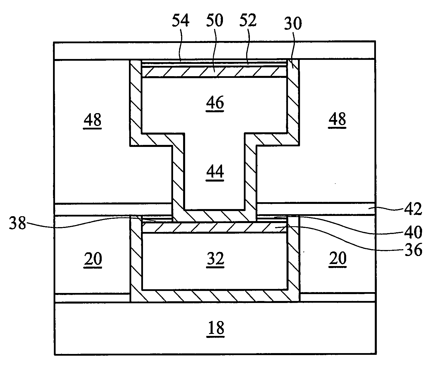
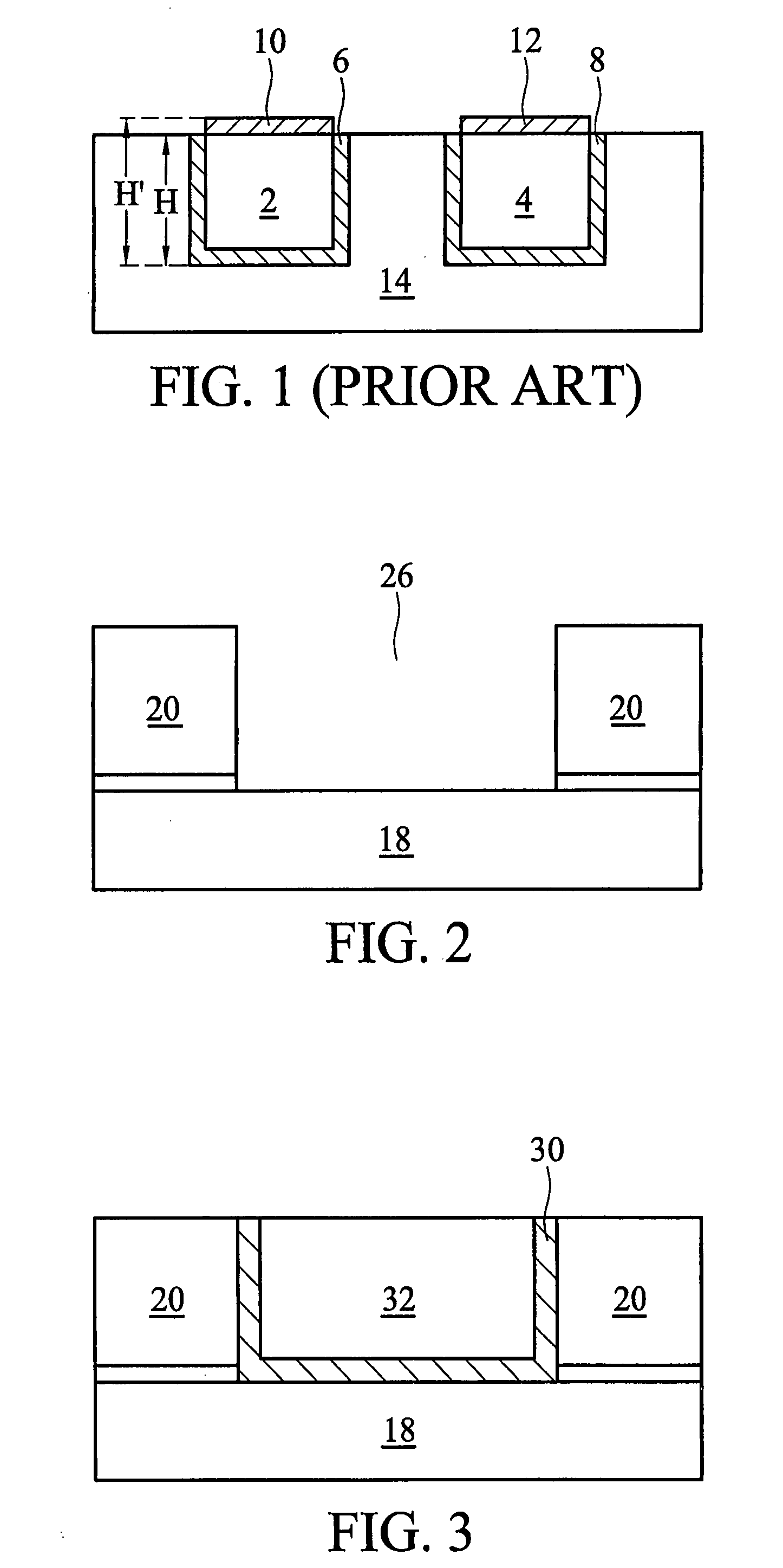
[0019]Interconnect structures comprising transitional interfaces between metal lines and overlying dielectric layers and methods of forming the same are provided. The intermediate stages of manufacturing an embodiment of the present invention are illustrated in FIGS. 2 through 8. Throughout the various views and illustrative embodiments of the present invention, like reference numbers are used to designate like elements.

[0020]FIG. 2 illustrates the formation of opening 26 in dielectric layer 20, which is formed over a schematically illustrated base layer 18. Base layer 18 may in


PUM


Abstract

An integrated circuit structure and methods for forming the same are provided. The integrated circuit structure includes a semiconductor substrate; a dielectric layer over the semiconductor substrate; an opening in the dielectric layer; a conductive line in the opening; a metal alloy layer overlying the conductive line; a first metal silicide layer overlying the metal alloy layer; and a second metal silicide layer different from the first metal silicide layer on the first metal silicide layer. The metal alloy layer and the first and the second metal silicide layers are substantially vertically aligned to the conductive line.

Description


Claims


Application Information

Patent Timeline
Owner TAIWAN SEMICON MFG CO LTD
Why Eureka
Try Eureka