Manufacturing method of high-linearity and high-power CMOS structure

a manufacturing method and high-power technology, applied in the direction of basic electric elements, electrical apparatus, semiconductor devices, etc., can solve the problems of increasing the dc power consumption of the cmos component, and achieve the effect of reducing leakage current and dc power consumption, increasing linearity and output power, and increasing output power

Inactive Publication Date: 2008-12-25
CHANG GUNG UNIVERSITY
View PDF1 Cites 4 Cited by
  • Summary
  • Abstract
  • Description
  • Claims
  • Application Information

AI Technical Summary

Benefits of technology

The present invention improves both radio frequency (R) performance by increasing its linearity while reducing energy usage due to reduced leaks or lowered voltage requirements for certain components such as amplifiers used during communication.

Problems solved by technology

This patented describes how traditional components like capacitors have limitations when trying to achieve better performance at higher frequencies for use within wireless technologies such as 5G or beyond. These issues include reduced signal-to-noise ratios due to increased impedance caused by metal interference from other parts around them. Additionally, there exist challenges related to improving RF Linearity and Power Loss Ratio (DC/R).

Method used


Image

  • Manufacturing method of high-linearity and high-power CMOS structure
  • Manufacturing method of high-linearity and high-power CMOS structure
  • Manufacturing method of high-linearity and high-power CMOS structure

Examples


Embodiment Construction

[0024]Now, the present invention will be described more specifically with reference to the following embodiments. It is to be noted that the following descriptions of preferred embodiments of this invention are, presented herein for purpose of illustration and description only; it is not intended to be exhaustive or to be limited to the precise form disclosed.

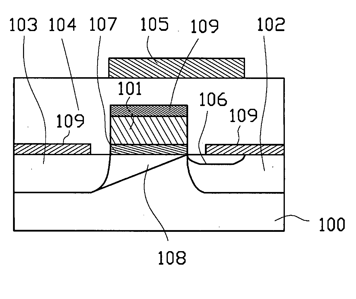
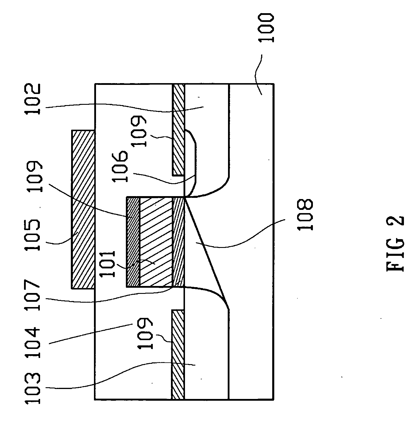
[0025]In an embodiment of this invention, a field plate technology is applied to a NMOS component in a standard TSMC 0.13 um CMOS process, in which, as shown in FIG. 2, the CMOS component is structured with a Si bulk as a base 100, comprising a gate 101 on a base 100, in which, a source 103 and a drain 102 are arranged in the base 100 between the two sides of the gate 101. Besides, a gate dielectric layer 107 is arranged between the gate 101 and the base 100, and may be made of silica and serve as an insulation layer that provides the CMOS component with an extremely high input resistance.

[0026]Further, metallic silicide layers 10


PUM


Abstract

This invention relates to a method for making a high-linearity and high-power CMOS structure and particularly to a field plate technology that is applied to a CMOS component, in which the field plate is formed on a dielectric layer of the CMOS, being arranged above a gate and a drain. An electric field is provided to significantly improve the RF linearity and output power of the CMOS component.

Description


Claims


Application Information

Patent Timeline
Owner CHANG GUNG UNIVERSITY
Why Eureka
Try Eureka