Semiconductor device including. multi-layer structure

a semiconductor and multi-layer technology, applied in the direction of semiconductor devices, basic electric elements, electrical equipment, etc., can solve the problems of high thermal budget, high leakage, and more problems in fabrication, and achieve high thermal budget, low oxidation reliability, and high leakage rate

Active Publication Date: 2015-06-18
MACRONIX INT CO LTD
View PDF7 Cites 1 Cited by
  • Summary
  • Abstract
  • Description
  • Claims
  • Application Information

AI Technical Summary

Benefits of technology

The technical effect of this patented method is that current methods for manufacturing 3D semiconductors have issues with reducing critical dimension size while maintaining good performance. This can lead to increased leakage currents, reduced thermal budgets, lower oxidation reliabilities, unwanted defects like poly bubble formation, and pealing off of conducting layers during production.

Problems solved by technology

The technical problem addressed in this patent is how to improve the performance and efficiency of 3D vertical gate (VG) type memories used in electronic systems such as computers or mobile phones.

Method used


Image

  • Semiconductor device including. multi-layer structure
  • Semiconductor device including. multi-layer structure
  • Semiconductor device including. multi-layer structure

Examples


Embodiment Construction

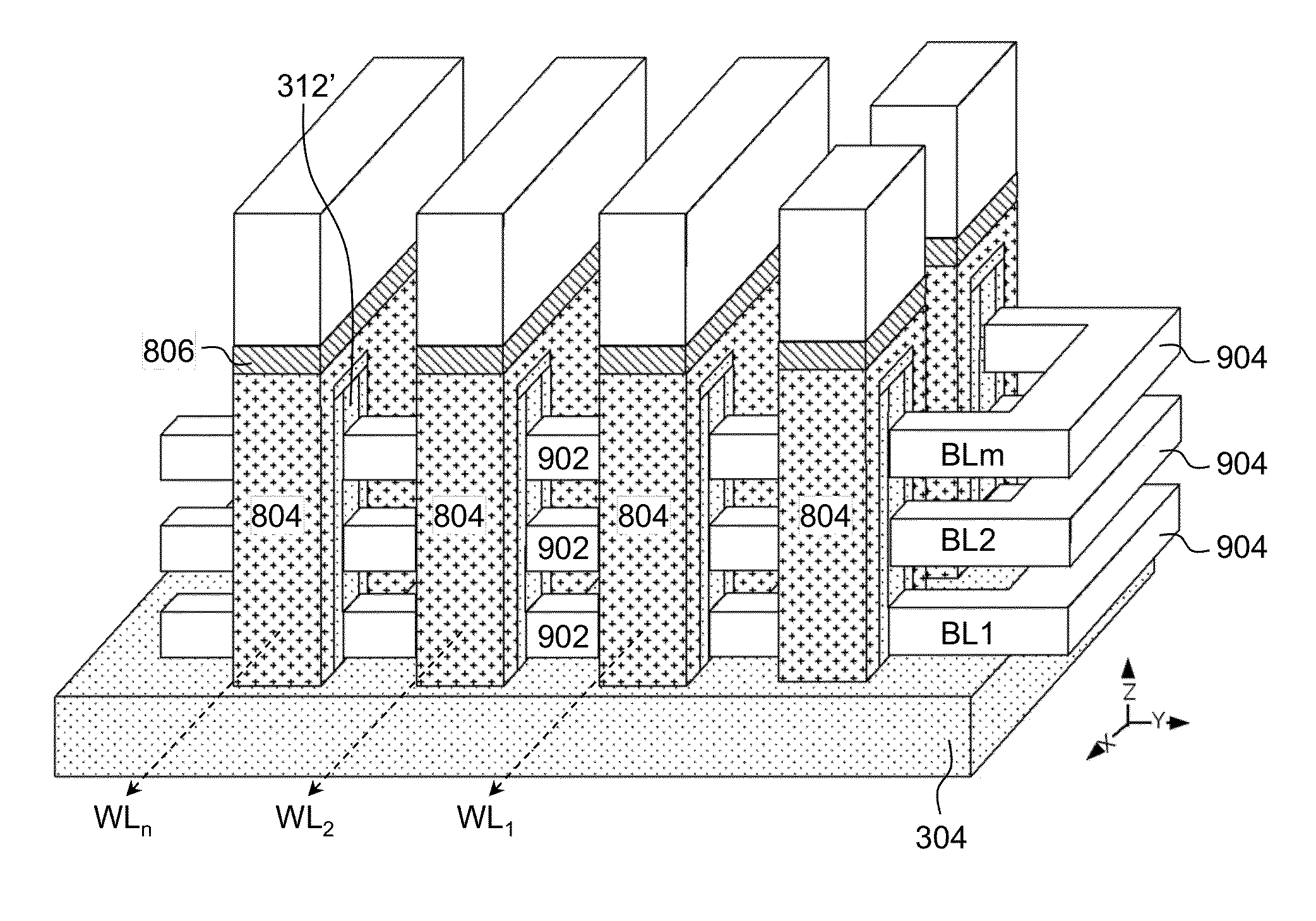
[0023]Example embodiments will now be described hereinafter with reference to the accompanying drawings, which form a part hereof, and which illustrate example embodiments which may be practiced. As used in the disclosures and the appended claims, the terms “example embodiment,”“exemplary embodiment,” and “present embodiment” do not necessarily refer to a single embodiment, although they may, and various example embodiments may be readily combined and / or interchanged without departing from the scope or spirit of example embodiments. Furthermore, the terminology as used herein is for the purpose of describing example embodiments only and is not intended to be limitations. In this respect, as used herein, the term “in” may include “in” and “on”, and the terms “a”, “an” and “the” may include singular and plural references. Furthermore, as used herein, the term “by” may also mean “from”, depending on the context. Furthermore, as used herein, the term “if” may also mean “when” or “upon”,


PUM


Abstract

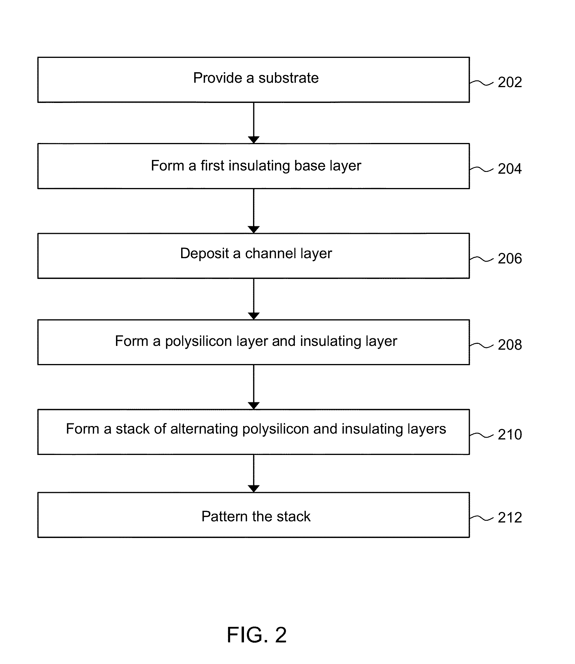
Present example embodiments relate generally to methods of fabricating a semiconductor device, and semiconductor devices thereof, comprising providing a substrate, forming an insulating base layer on the substrate, and disposing a conductive layer on the insulating base layer at an initial temperature. The methods further comprise increasing the initial temperature at a first increase rate to a first increased temperature and performing an in-situ annealing process to the conductive layer at the first increased temperature. The methods further comprise increasing the first increased temperature at a second increase rate to a second increased temperature, and forming an insulating layer after performing the in-situ annealing process at the second increased temperature.

Description


Claims


Application Information

Patent Timeline
Owner MACRONIX INT CO LTD
Why Eureka
Try Eureka