OLED display substrate and manufacture method thereof

a technology of oled and display substrate, which is applied in the direction of basic electric elements, electrical apparatus, and semiconductor devices, can solve the problems of inability to light oled, and achieve the effect of simple manufacturing method

Active Publication Date: 2016-11-24
SHENZHEN CHINA STAR OPTOELECTRONICS TECH CO LTD
View PDF3 Cites 5 Cited by
  • Summary
  • Abstract
  • Description
  • Claims
  • Application Information

AI Technical Summary

Benefits of technology

The technical effect of this patented technology is that it provides an OLED display substrate with improved resistance against short circuits caused by electrodes on its surface. This prevents damage from over-current flow and maintains proper light output for longer periods of time.

Problems solved by technology

This patent describes different technical problem addressed in this patent: The technical problem presented in this patent text relates to improving the performance and functionality of OLED display panels while reducing their size and weight. Current techniques such as PassiveMatrix OLED (AMLCD) and Active Matrix OLED (AMOLED) require expensive equipment and complicated processes that limit their use. Therefore, there is a need for new technologies that improve these characteristics without requiring expensive equipment.

Method used


Image

  • OLED display substrate and manufacture method thereof
  • OLED display substrate and manufacture method thereof
  • OLED display substrate and manufacture method thereof

Examples


Embodiment Construction

[0041]For better explaining the technical solution and the effect of the present invention, the present invention will be further described in detail with the accompanying drawings and the specific embodiments.

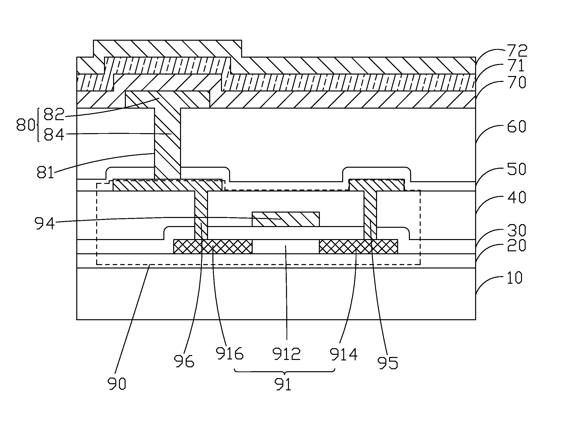
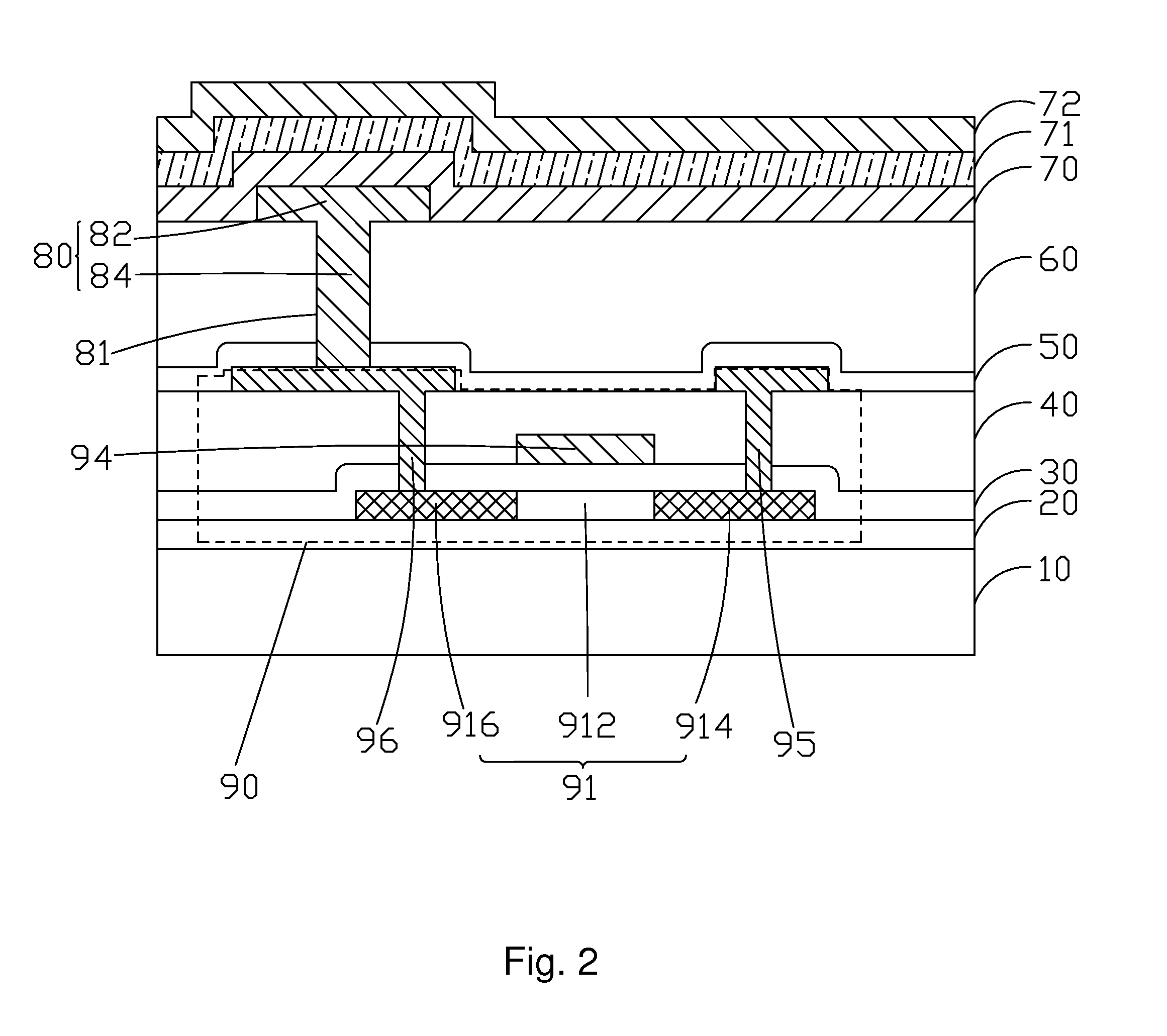
[0042]Please refer to FIG. 2. The present invention first provides an OLED display substrate, comprising:

[0043]a substrate 10, and the substrate 10 is a transparent substrate, and preferably, the substrate 10 is a glass substrate;

[0044]a TFT 90 located on the substrate 10; specifically, the TFT 90 comprises: a buffer layer 20 located on the substrate 10, a channel area 912 and a semiconductor layer 91 located in a source area 912 and a drain area 914 respectively at two sides of the channel area 912 on the buffer layer 20, a gate isolation layer 30 located on the semiconductor layer 91, a gate 94 located above the channel area 912 and on the gate isolation layer 30, an interlayer insulation layer 40 on the gate 94, a source 95 located in the source area 914 and penetrating the ga


PUM


Abstract

The present invention provides an OLED display substrate and a manufacture method thereof. The OLED display substrate comprises a substrate (10), a TFT (90) located on the substrate (10), a passivation layer (50) located on the TFT (90), a flat layer (60) located on the passivation layer (50), a connecting electrode (80) being located on the flat layer (60) and contacting the TFT (90), an anode (70) being located on the flat layer (60) and covering the connecting electrode (80), an organic emitting layer (71) located on the anode (70) and a cathode (72) located on the organic emitting layer (71); the connecting electrode (80) contacts the TFT (90) via the contact hole (81) penetrating the flat layer (60) and the passivation layer (50); the anode (70) is electrically connected to the TFT (90) via the connecting electrode (80); the short circuit between the cathode and anode of the OLED display substrate can be prevented for avoiding the current concentration and ensuring the normal illumination of the OLED.

Description


Claims


Application Information

Patent Timeline
Owner SHENZHEN CHINA STAR OPTOELECTRONICS TECH CO LTD
Why Eureka
Try Eureka