Reverse-conducting insulated-gate bipolar transistor structure and corresponding fabrication method thereof
- Summary
- Abstract
- Description
- Claims
- Application Information
AI Technical Summary
Benefits of technology
Problems solved by technology
Method used
Image

Examples
Example
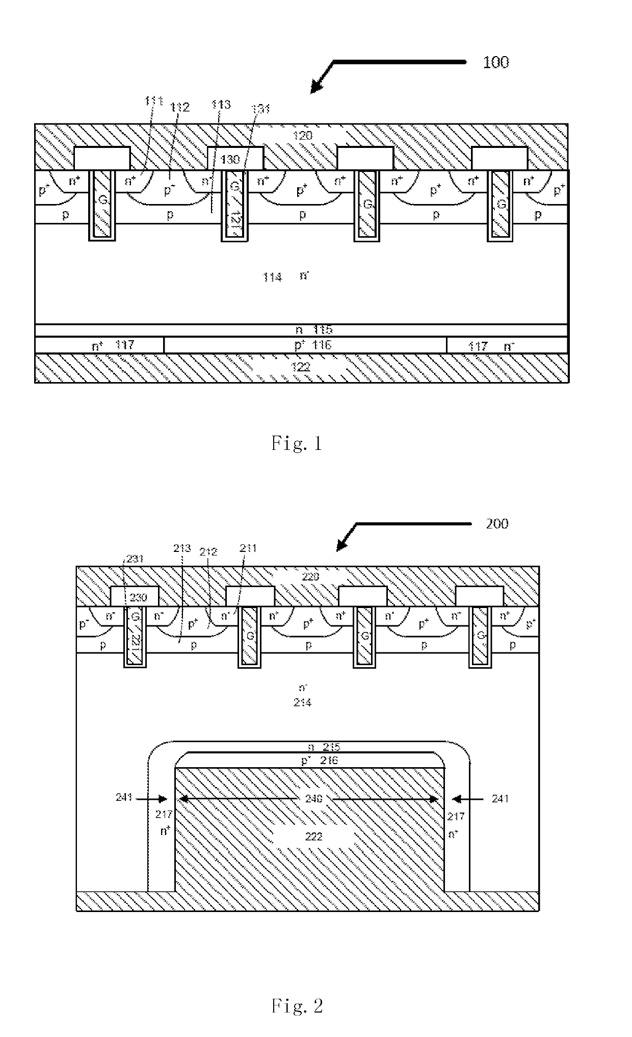
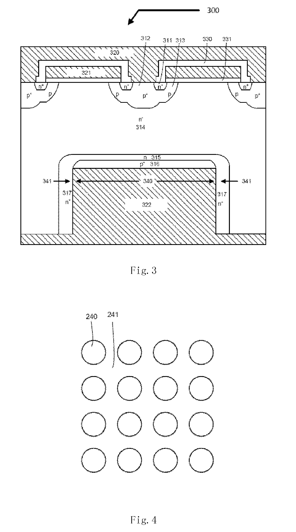
[0059]In the present invention, an n channel device is used to perform description. However, it should be understood that in the following descriptions that the present invention is similarly applicable to a p channel device. In the specification of the present invention, a heavily doped n− type region is marked as n+, and a heavily doped p-type region is marked as p+. Unless otherwise indicated, in silicon, a heavily doped region usually has a doping concentration between 1×1019 cm−3 and 1×1021 cm−3. In the specification of the present invention, a lightly doped n− type region is marked as n−, and a lightly doped p-type region is marked as p−. Unless otherwise indicated, in silicon, a lightly doped region usually has a doping concentration between 1×1013 cm−3 and 1×1017 cm−3.
[0060]FIG. 2 is a cross-sectional view of the present invention implemented in a trench gate RC-IGBT device 200. The device 200 includes: an emitter electrode (220) at the front surface; a plurality of cell struct
PUM
 Abstract
Description
Claims
Application Information
 - R&D Engineer
- R&D Manager
- IP Professional
- Industry Leading Data Capabilities
- Powerful AI technology
- Patent DNA Extraction
Browse by: Latest US Patents, China's latest patents, Technical Efficacy Thesaurus, Application Domain, Technology Topic.
© 2024 PatSnap. All rights reserved.Legal|Privacy policy|Modern Slavery Act Transparency Statement|Sitemap