Semiconductor device and method of manufacturing semiconductor device

a semiconductor and semiconductor technology, applied in the direction of semiconductor devices, semiconductor/solid-state device details, radiation controlled devices, etc., can solve the problems of mtj element characteristics degradation, achieve low heat resistance, reduce thermal budget, and avoid element characteristics from being degraded

Pending Publication Date: 2019-11-28
SONY SEMICON SOLUTIONS CORP
View PDF5 Cites 4 Cited by
  • Summary
  • Abstract
  • Description
  • Claims
  • Application Information

AI Technical Summary

Benefits of technology

The technical effect addressed in this patented technology relates to improving the performance of magnetoresistive random access memories used in electronic devices without compromizing their ability to maintain data integrity over time or reducing power consumption. By incorporating these elements into the design of the chip itself instead of just adding them afterwards, we can improve overall functionality while minimizing impacts upon other parts within the integrated circuits themselves.

Problems solved by technology

The technical problem addressed in this patents relates to reducing damage caused when conducting electrical connections between different layers within electronic devices such as integrated circuits or cameras used with imagers.

Method used


Image

  • Semiconductor device and method of manufacturing semiconductor device
  • Semiconductor device and method of manufacturing semiconductor device
  • Semiconductor device and method of manufacturing semiconductor device

Examples


second embodiment (

2. Second Embodiment (An example semiconductor device including three substrates laminated together)

3. Modification Example 1 (An example in which a leading electrode is further provided on the surface S2 of the second substrate)

third embodiment (

4. Third Embodiment (An example semiconductor device provided with a circuit having a communication function on the first substrate)

5. Modification Example 2 (An example in which an antenna is further provided in addition to the circuit having the communication function)

first embodiment

(1-1 Configuration of Semiconductor Device)

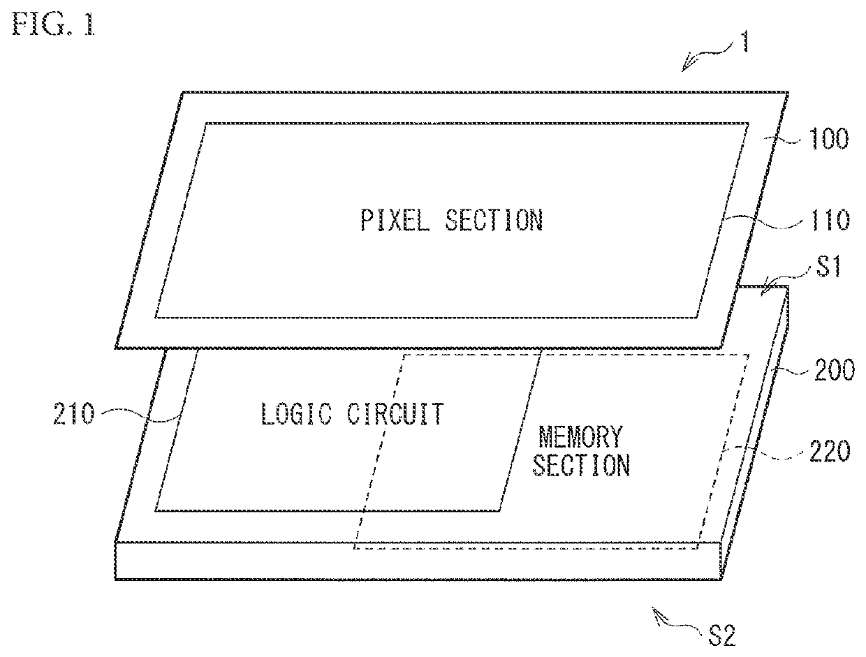
[0035]FIG. 1 illustrates a schematic configuration of a semiconductor device (semiconductor device 1) according to a first embodiment of the present disclosure. The semiconductor device 1 includes a first substrate 100 and a second substrate 200 electrically coupled to each other and laminated together. The semiconductor device 1 is, for example, a laminated image sensor, in which the first substrate 100 is provided with a pixel section 110 and the second substrate 200 is provided with a logic circuit 210 and a memory section 220. In the present embodiment, the logic circuit 210 is provided on a surface (first surface, surface S1), of the second substrate, facing the first substrate 100, and the memory section 220 is provided on a surface (second surface, surface S2), of the second substrate 200, opposite to the surface facing the first substrate 100.

[0036]Unit pixels are two-dimensionally arranged on the pixel section 110 of the first substra


PUM


Abstract

A semiconductor device according to an embodiment of the present disclosure includes: a first substrate provided with an active element; and a second substrate laminated with the first substrate and electrically coupled to the first substrate, in which the second substrate is provided with a first transistor configuring a logic circuit on a first surface and with a non-volatile memory element on a second surface opposite to the first surface.

Description


Claims


Application Information

Patent Timeline
Owner SONY SEMICON SOLUTIONS CORP
Why Eureka
Try Eureka