Wired circuit board and producing method thereof
- Summary
- Abstract
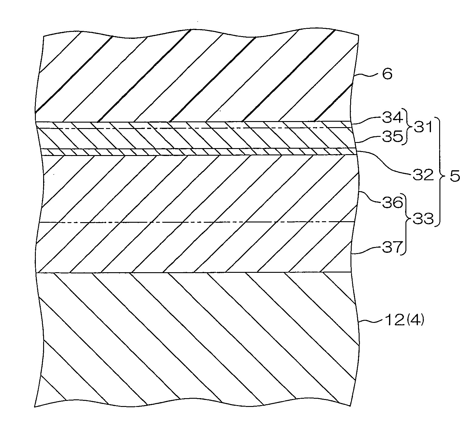
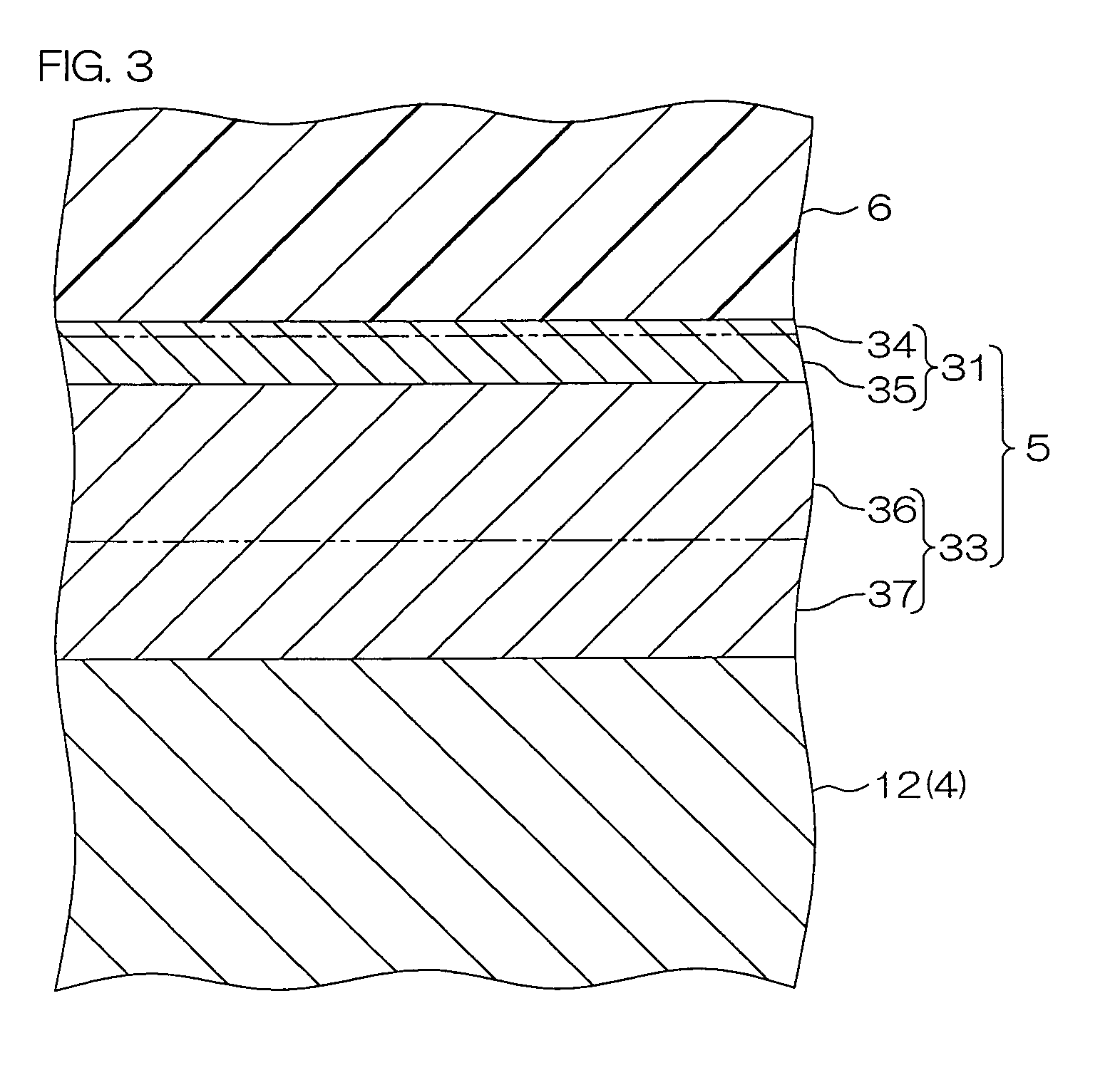
- Description
- Claims
- Application Information
AI Technical Summary
Benefits of technology
Problems solved by technology
Method used
Image

Examples
Example
Example 1
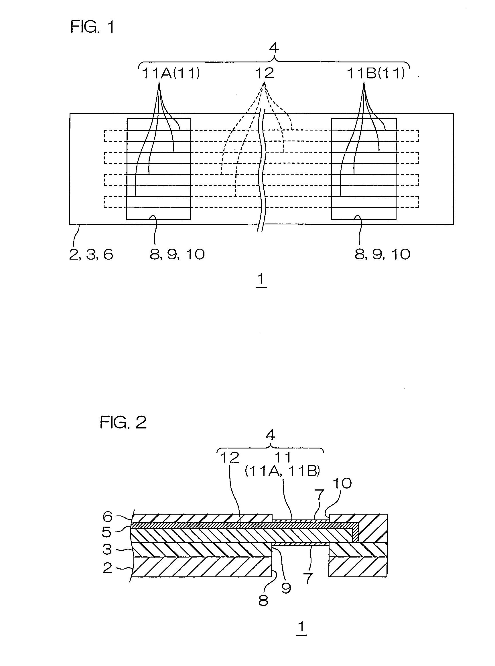
[0138]A metal supporting board made of a stainless steel (SUS304) foil with a thickness of 20 μm was prepared (see FIG. 4(a)).
[0139]Then, a solution of a photosensitive polyamic acid resin was uniformly coated on the entire surface of the metal supporting board, and dried by heating at 90° C. to form a base coating. Subsequently, the base coating was exposed to light via a photomask, developed, and then cured (imidized) by heating at 370° C. to form an insulating base layer made of polyimide with a thickness of 10 μm on the metal supporting board (see FIG. 4(b)).
[0140]Then, a chromium thin film with a thickness of 50 nm and a copper thin film with a thickness of 100 nm were successively formed on the entire surface of the insulating base layer by a sputter deposition method to form a seed film. Subsequently, on the upper surface of the seed film, a plating resist in a pattern reverse to a conductive pattern was formed, and then the conductive pattern made of copper with a thi
Example
Examples 2 to 5
[0149]Suspension boards with circuit were obtained in the same manner as in EXAMPLE 1 except that the thickness of the tin layer (the thickness of the tin layer before the heating step) was changed to the values in the parentheses in Table 1.
Example
Examples 6 to 10
[0150]Suspension boards with circuit were obtained by forming tin-based thin layers in the same manner as in EXAMPLE 1 except that a third cooling step in vacuum and a re-heating step under an atmospheric pressure were performed instead of performing the first cooling step in vacuum and the second cooling step under an atmospheric pressure.
[0151]That is, in the third cooling step after the heating step, the suspension boards with circuit in the process of production which included tin alloy layers were cooled in vacuum (1 Pa) from 400° C. to 25° C. by stopping the operation of the heater, while continuing the operation of the vacuum pump of the reduced-pressure drier used in the heating step. A cooling rate in the third cooling step was 3° C. per minute.
[0152]In the re-heating step after the third cooling step, the suspension boards with circuit were each loaded in another drier, and heated under an atmospheric pressure for 30 minutes to 200° C. at a heating rate of 10
PUM
| Property | Measurement | Unit |
|---|---|---|
| Temperature | aaaaa | aaaaa |
| Temperature | aaaaa | aaaaa |
| Thickness | aaaaa | aaaaa |
Abstract
Description
Claims
Application Information
 - R&D Engineer
- R&D Manager
- IP Professional
- Industry Leading Data Capabilities
- Powerful AI technology
- Patent DNA Extraction
Browse by: Latest US Patents, China's latest patents, Technical Efficacy Thesaurus, Application Domain, Technology Topic.
© 2024 PatSnap. All rights reserved.Legal|Privacy policy|Modern Slavery Act Transparency Statement|Sitemap