Low-temperature formation method for emitter tip including copper oxide nanowire or copper nanowire and display device or light source having emitter tip manufactured using the same

Inactive Publication Date: 2006-05-09
SEOUL NAT UNIV R&DB FOUND
View PDF13 Cites 6 Cited by
  • Summary
  • Abstract
  • Description
  • Claims
  • Application Information

AI Technical Summary

Benefits of technology

[0013]The reduction gas or a plasma generating gas can be a H2 gas.
[0014]According to another embodiment of the present invention, there is provided a display device or a light source

Problems solved by technology

Unless a glass substrate is used, the manufacture of carbon nanotubes is very likely to have technical and economical problems.
Although there are known methods for lowering a formation temperature of carbon nanotubes to a temperatur

Method used


Image

  • Low-temperature formation method for emitter tip including copper oxide nanowire or copper nanowire and display device or light source having emitter tip manufactured using the same
  • Low-temperature formation method for emitter tip including copper oxide nanowire or copper nanowire and display device or light source having emitter tip manufactured using the same
  • Low-temperature formation method for emitter tip including copper oxide nanowire or copper nanowire and display device or light source having emitter tip manufactured using the same

Examples


first embodiment

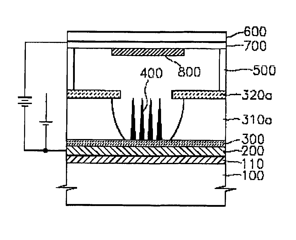
[0051]FIGS. 7 through 9 are cross-sectional views illustrating a method of manufacturing an FED using the low-temperature formation method for emitter tips including copper oxide nanowires or copper nanowires according to the present invention, according to another embodiment of the present invention. The same formation methods, thickness, shape, size, and material of elements as in the first embodiment will not be repeated here.

[0052]Referring to FIG. 7, unlike in the first embodiment, before a copper layer is formed, a cathode electrode 200, an insulating layer 310, a metal layer 320 for a gate electrode, and a photoresist pattern PR are sequentially formed on a large-sized lower substrate 100. The metal layer 320 for the gate electrode and the insulating layer 310 are sequentially etched using the photoresist pattern PR as an etch mask, thereby forming a gate electrode 320a and an insulating pattern 310a. As a result, the surface of the cathode electrode 200 is exposed.

[0053]Referri

third embodiment

[0060]FIGS. 12 through 14 are cross-sectional views illustrating a method of manufacturing a white light source using the low-temperature formation method of the present invention, according to further another embodiment of the present invention. The present embodiment differs from the third embodiment in that emitter tips 400 are grouped into several groups and each group constitutes one cell.

[0061]Referring to FIG. 12, a first insulating layer 110, a cathode electrode 200, a copper layer 300, and a second insulating layer 310 are sequentially formed on a lower substrate 100 and patterned using photolithography and etching processes, thereby forming a second insulating pattern 310a. The second insulating pattern 310a defines a plurality of holes H, which expose the copper layer 300. Here, the second insulating pattern 310a is formed such that each of the holes H has a diameter and an interval suitable for defining a cell.

[0062]Referring to FIG. 13, copper oxide nanowires are formed us


PUM


Abstract

Provided are a low-temperature formation method for emitter tips including copper oxide nanowires or copper nanowires and a display device or a light source manufactured using the same. The low-temperature formation method includes preparing a substrate having an exposed copper surface. The copper surface contacts an oxide solution at a low temperature of 100° C. or less to grow copper oxide nanowires on the surface of the substrate. Optionally, a reduction gas or a heat is supplied to the copper oxide nanowires, or plasma processing is performed on the copper oxide nanowires, thereby reducing the copper oxide nanowires to copper nanowires. Thus, emitter tips including copper oxide nanowires or copper nanowires are formed densely at a low temperature such that the emitter tips have a shape and length suitable for emission of electrons.

Description


Claims


Application Information

Patent Timeline
Owner SEOUL NAT UNIV R&DB FOUND
Why Eureka
Try Eureka