Memory cell that includes a carbon nano-tube reversible resistance-switching element and methods of forming the same

A technology of memory cells and carbon nanotubes, used in electrical components, static memory, digital memory information, etc.

Active Publication Date: 2011-04-20
SANDISK TECH LLC
View PDF12 Cites 0 Cited by
  • Summary
  • Abstract
  • Description
  • Claims
  • Application Information

AI Technical Summary

Problems solved by technology

[0005] However, fabricating memory devices from CNT materials is technically challen

Method used


Image

  • Memory cell that includes a carbon nano-tube reversible resistance-switching element and methods of forming the same
  • Memory cell that includes a carbon nano-tube reversible resistance-switching element and methods of forming the same
  • Memory cell that includes a carbon nano-tube reversible resistance-switching element and methods of forming the same

Examples


Embodiment Construction

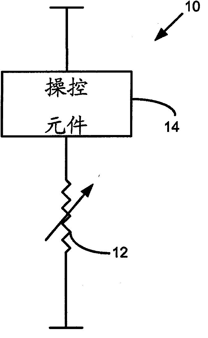
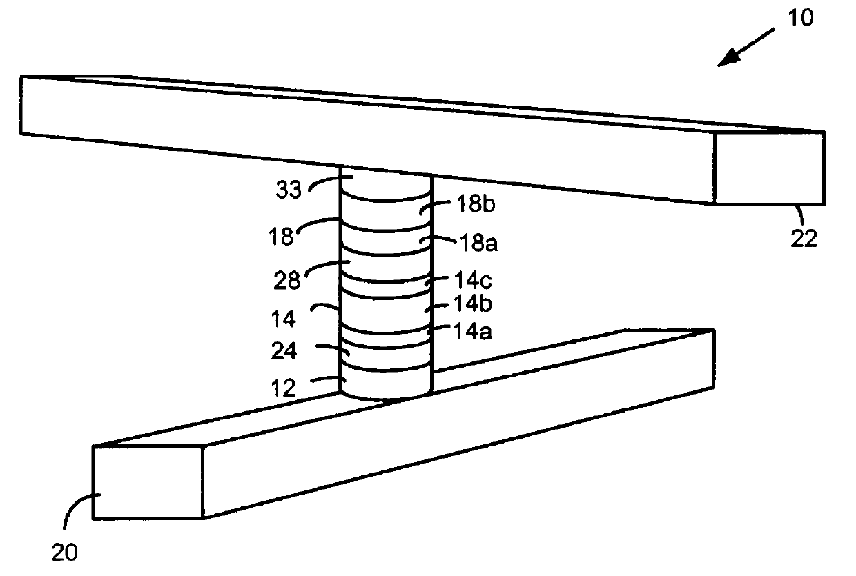
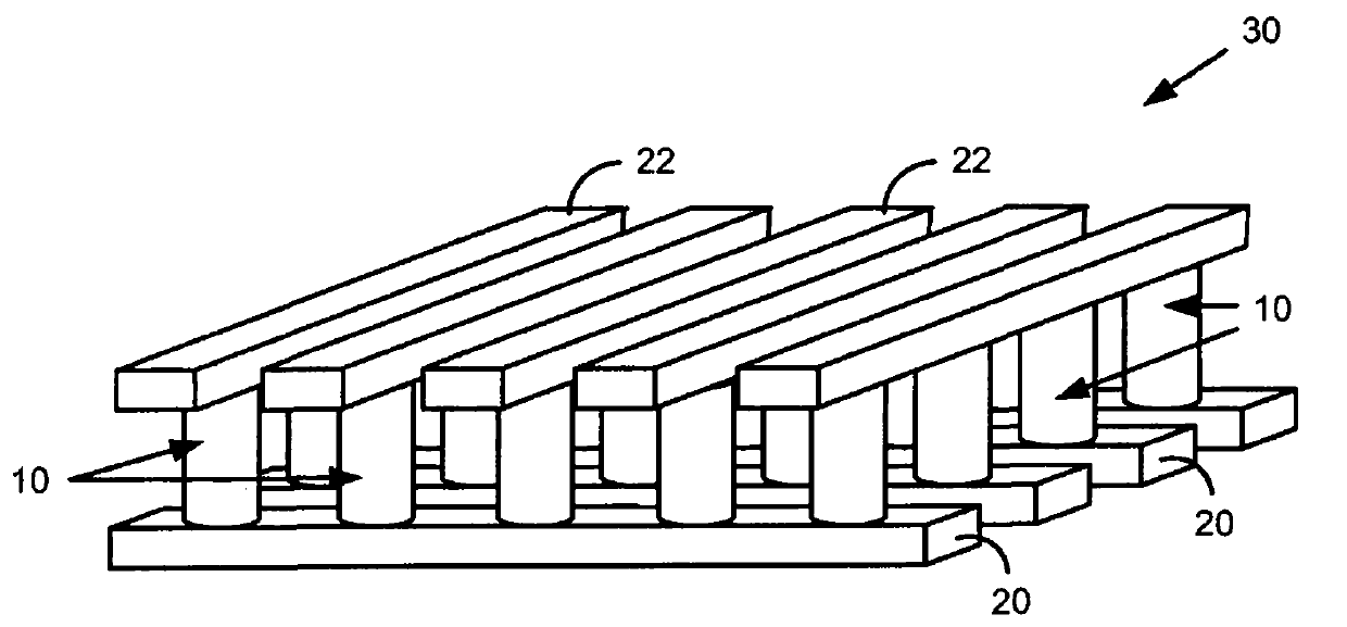
[0018] Some CNT materials have been shown to exhibit reversible resistance-switching properties that may be suitable for use in non-volatile memory. However, when CNT materials are used in forming memory cells, the deposited or grown CNT materials typically have rough surface topography, and significant thickness variations, such as many peaks and valleys. The rough surface topography of CNT material can cause difficulties in forming memory cells. For example, the rough surface topography of CNT materials may make the CNT materials difficult to etch without overetching the underlying substrate, increasing manufacturing costs and complexity associated with their use in integrated circuits. Additionally, voids in the surface of the CNT material may be penetrated by conductive material deposited over the CNT material and cause vertical shorts to occur. Although the peaks on the surface of the CNT material can be removed by planarization, any valleys or voids that remain after plana


PUM


Abstract

Methods of forming planar carbon nanotube (''CNT'') resistivity-switching materials for use in memory cells are provided, that include depositing first dielectric material (58b), patterning the first dielectric material, etching the first dielectric material to form a feature within the first dielectric material, depositing CNT resistivity-switching material over the first dielectric material to fill the feature at least partially with the CNT resistivity-switching material, depositing second dielectric material (112) over the CNT resistivity-switching material, and planarizing the second dielectric material and the CNT resistivity-switching material so as to expose at least a portion of the CNT resistivity-switching material within the feature. Other aspects are also provided.

Description


Claims


Application Information

Patent Timeline
Owner SANDISK TECH LLC
Why Eureka
Try Eureka