Preparation method of antireflection film allowing wide-angle incidence of infrared optical waveband in silicon or germanium base
A technology in infrared optics and substrates, used in sputtering, ion implantation, metal material coating, etc. The problems of reduced capacity, difficult film system design and process, etc., can achieve the effect of high film layer firmness and high density, temperature shock resistance, deliquescence resistance and laser damage resistance, and high density.
- Summary
- Abstract
- Description
- Claims
- Application Information
AI Technical Summary
Problems solved by technology
Method used
Image

Examples
Example Embodiment
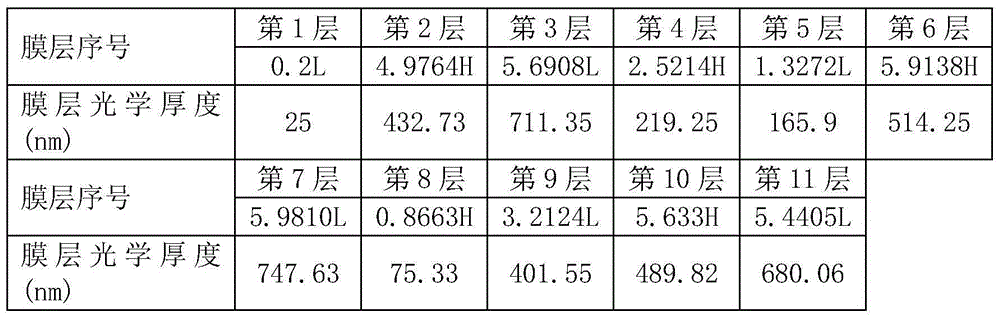
[0021] Example 1
[0022] According to the present invention, the advanced optical film design software (TFCalc) of the United States is first used to design an optimized film system that meets the technical specifications of the present invention. The optically processed silicon material is used as the substrate to coat the surface, and the film system design formula: G / 0.2L(5H5L)^50.2L / Air is used to optimize the calculation of the optical thickness value of each film and column grids in order. Where G is the base of silicon material and L is the refractive index N L = 1.60 Al 2 O 3 Film material, H is the refractive index N H = 2.20 ZnS film material, Air is the refractive index N A =1 air medium, film reference wavelength λ c = 800nm. The above H and L are granular membrane materials with a purity of 99.9%. The specific steps include:
[0023] (1) Using silicon or germanium material as the base and insulating the surface of the silicon or germanium material from contact with
Example Embodiment
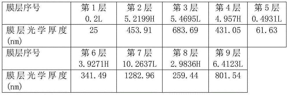
[0050] Example 2
[0051] According to the calculated and designed optical thickness values of each layer of the 9-layer film in Table 2 below, the method of Experimental Example 1 was repeated, using the optimized film formula of the present invention and the optical thickness of each layer in Table 2, in the coating process steps:
[0052] (1) Repeat the process step (1) in Example 1;
[0053] (2) Repeat the process step (2) in Example 1;
[0054] (3) Repeat the process step (3) in Example 1;
[0055] (4) Repeat the process step (4) in Example 1;
[0056] (5) Repeat the process step (5) in Example 1;
[0057] The actual optical thickness of each layer recorded after coating is shown in Table 2:
[0058] Table 2 (The optical thickness value table of the 9-layer germanium film actually plated in Example 2)
[0059]
[0060] Note: The value after the decimal point is not taken because the accuracy is sufficient to reach the design scheme.
[0061] (6) Annealing treatment: repeat the process st
PUM
 Abstract
Description
Claims
Application Information
 - R&D Engineer
- R&D Manager
- IP Professional
- Industry Leading Data Capabilities
- Powerful AI technology
- Patent DNA Extraction
Browse by: Latest US Patents, China's latest patents, Technical Efficacy Thesaurus, Application Domain, Technology Topic.
© 2024 PatSnap. All rights reserved.Legal|Privacy policy|Modern Slavery Act Transparency Statement|Sitemap